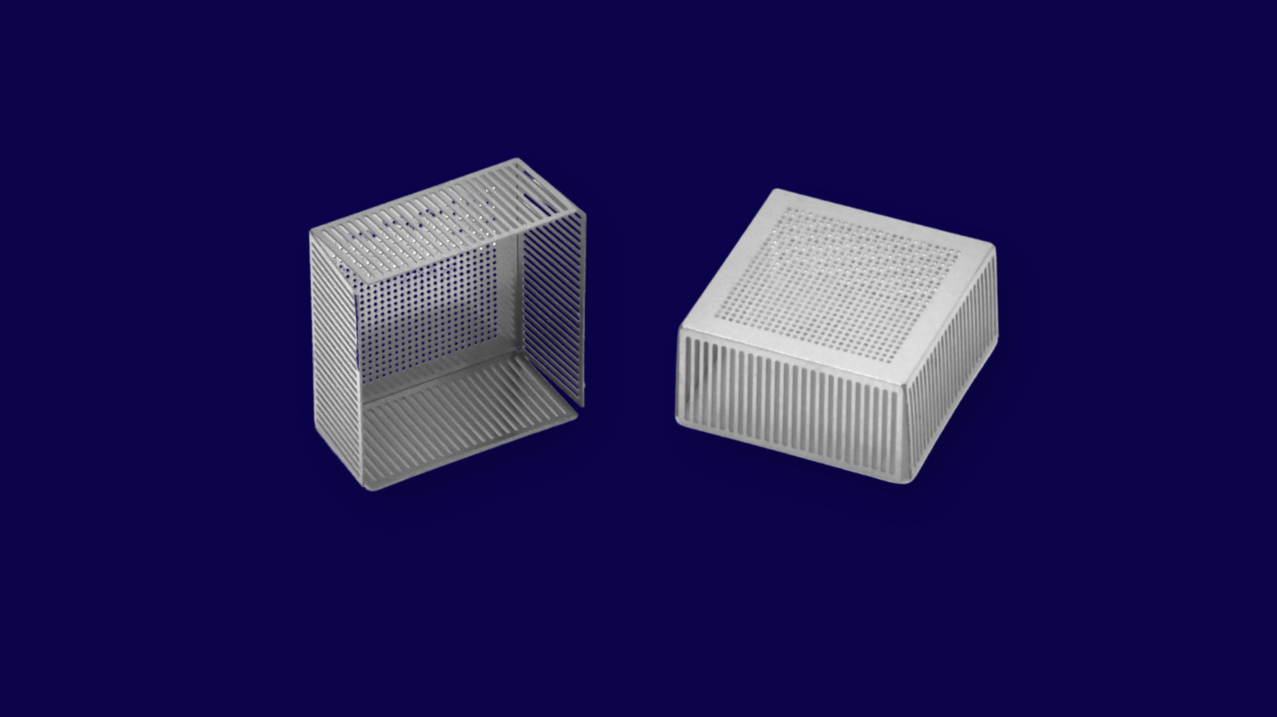
RF Shielding Design Guide: Tips for Engineers and Product Designers
Learn key RF shielding design tips for engineers and product designers. Discover how E-Fab helps create EMI-compliant, high-performance electronic devices.

Learn key RF shielding design tips for engineers and product designers. Discover how E-Fab helps create EMI-compliant, high-performance electronic devices.
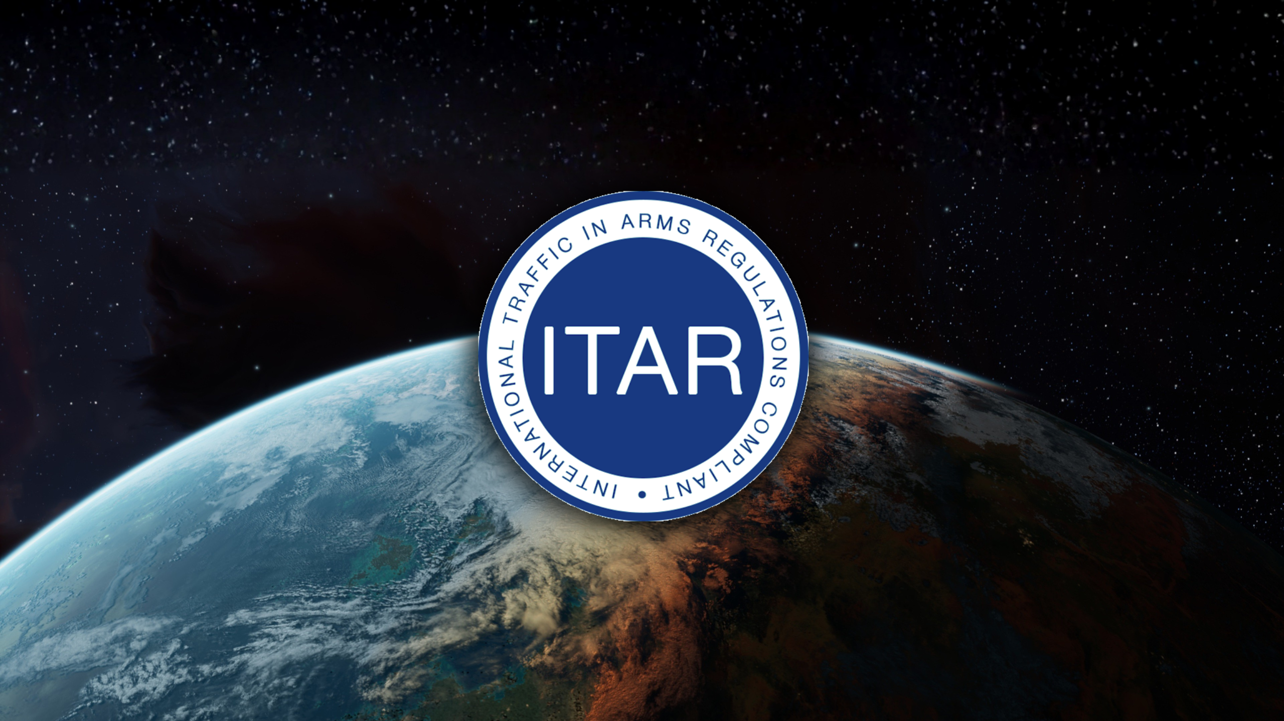
Learn why ITAR compliance matters in aerospace and defense manufacturing. Discover how E-Fab, an ITAR-registered manufacturer, safeguards sensitive data and ensures full regulatory compliance.
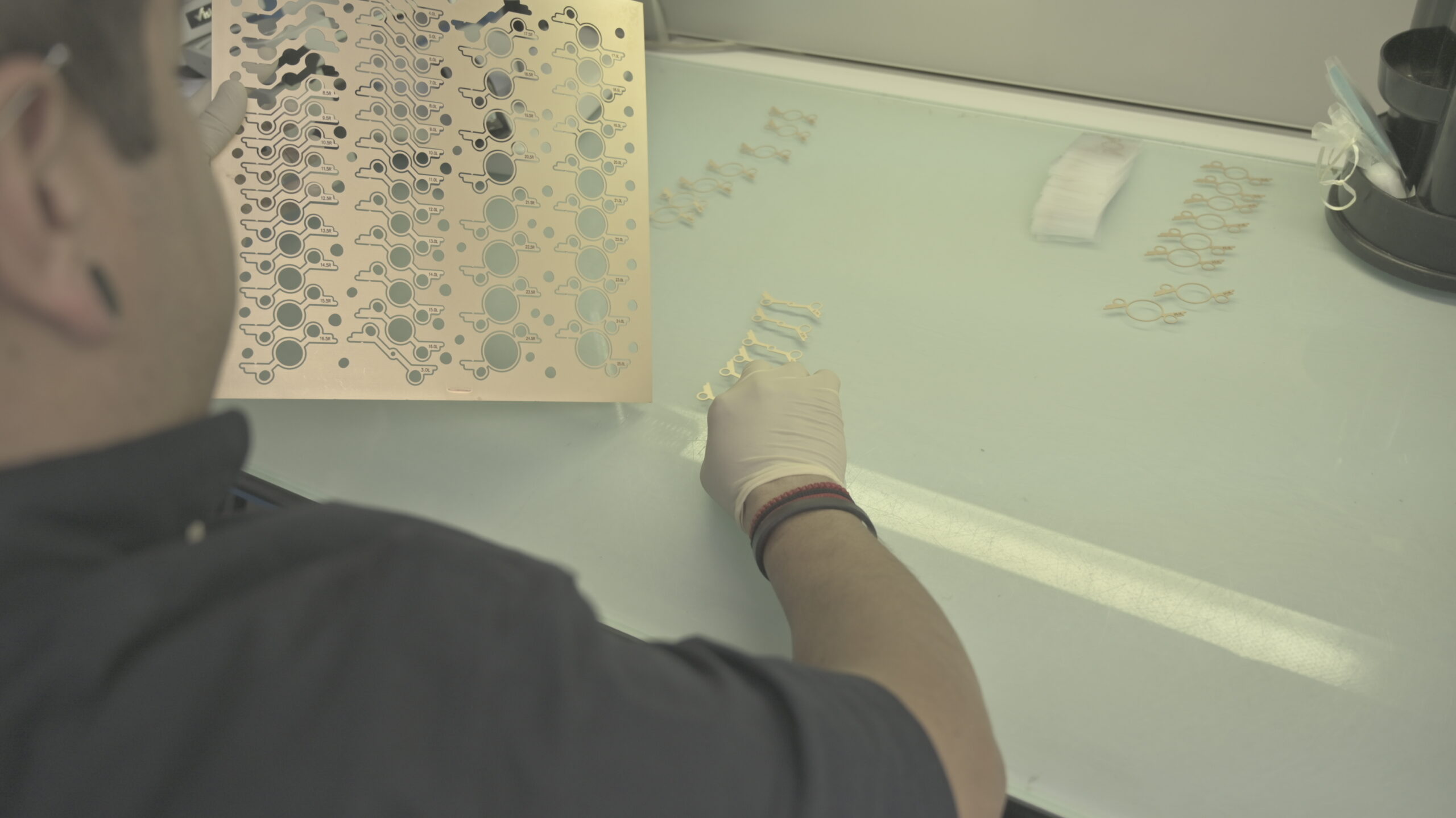
Explore effective techniques for thin metal etching in precision manufacturing. Enhance your skills and improve your production quality. Read more now.
Explore efficient semiconductor manufacturing processes with key insights that can enhance productivity and reduce waste. Read the article to learn more.
Explore the best EMI shielding materials for effective protection. Make informed choices to reduce interference—read the article for essential insights.

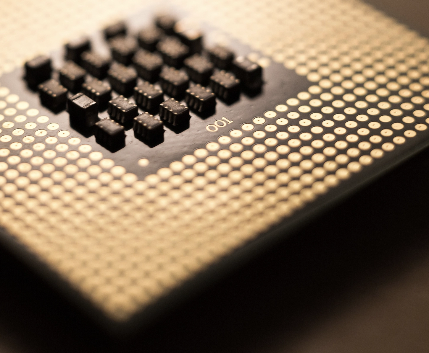
Explore the applications and advantages of photochemical etching and diffusion bonding. Learn how these precision manufacturing processes complement each other to achieve high-integrity components. Read more!
Explore the applications and advantages of photochemical etching and diffusion bonding. Learn how these precision manufacturing processes complement each other to achieve high-integrity components. Read more!

Explore the performance and challenges of aerospace screens in this insightful article. Discover key factors influencing their effectiveness. Read more now!
Explore the performance and challenges of aerospace screens in this insightful article. Discover key factors influencing their effectiveness. Read more now!
Explore the applications and advantages of photochemical etching and diffusion bonding. Learn how these precision manufacturing processes complement each other to achieve high-integrity components. Read more!