Photo Etching on Metal: Parts for Semiconductor Equipment – Lead Frames, Bus Bars & Bipolar Plates
Burr-free, stress-free precision photo-etched components — lead frames, etched bus bars, bipolar plates, and RF shielding — manufactured to tight tolerances from prototype through production.
Precision Photo-Etched Components for Semiconductor Equipment
Semiconductor equipment manufacturers require precision metal components capable of maintaining tight tolerances, dimensional consistency, and repeatable performance across demanding production environments. As semiconductor devices continue to evolve toward smaller geometries and higher-performance architectures, component manufacturers face increasing pressure to deliver burr-free, fine-feature metal parts without distortion or material degradation.
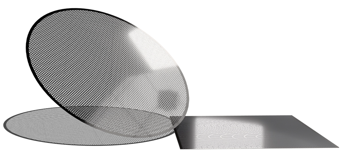
E-Fab manufactures high-precision photo-etched metal components for semiconductor equipment and advanced electronics applications, including lead frames, etched bus bars, bipolar plates, RF shielding components, and precision conductive interconnects. Using the photo etching process, which uses light and acid instead of mechanical saws, lasers, or stamping dies, E-Fab starts with a metal sheet coated with a light-sensitive photoresist, exposes it to ultraviolet light to form a protective pattern, and then sprays the developed sheet with an etching solution to produce burr-free etched metal components with no heat-affected zone (HAZ), sub-micron pattern fidelity, and repeatable dimensional control from prototype through production.
For semiconductor applications where stamping introduces burrs and laser cutting creates heat-affected zones, photochemical etching provides a manufacturing solution in which the etchant solution dissolves unprotected areas and preserves the original magnetic, electrical, and tensile properties of the metal while producing intricate geometries and thin-metal semiconductor components without secondary deburring or material distortion.
As semiconductor reshoring initiatives and CHIPS Act-related investments continue expanding U.S.-based manufacturing capacity, demand for precision etched semiconductor components continues to accelerate across semiconductor packaging, RF shielding, power electronics, and fuel cell technologies.
Precision Semiconductor Component Types
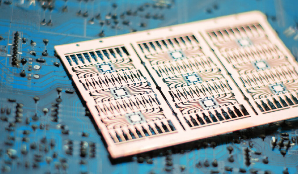
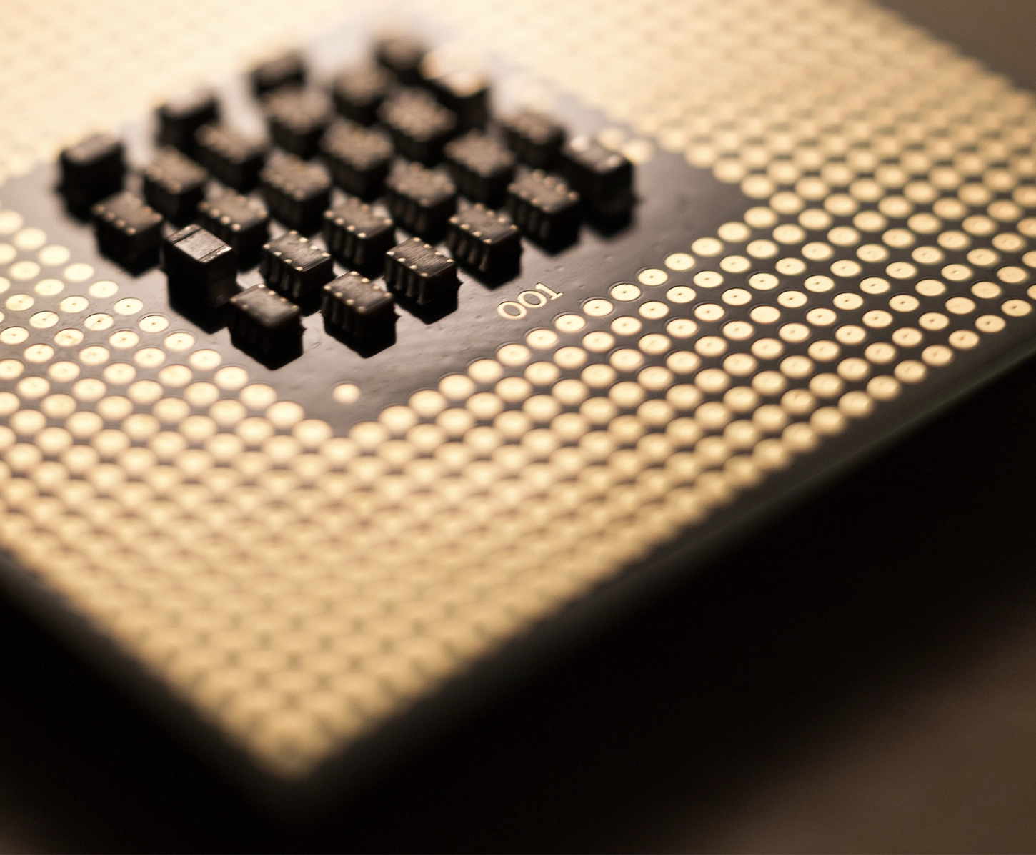
Lead Frames
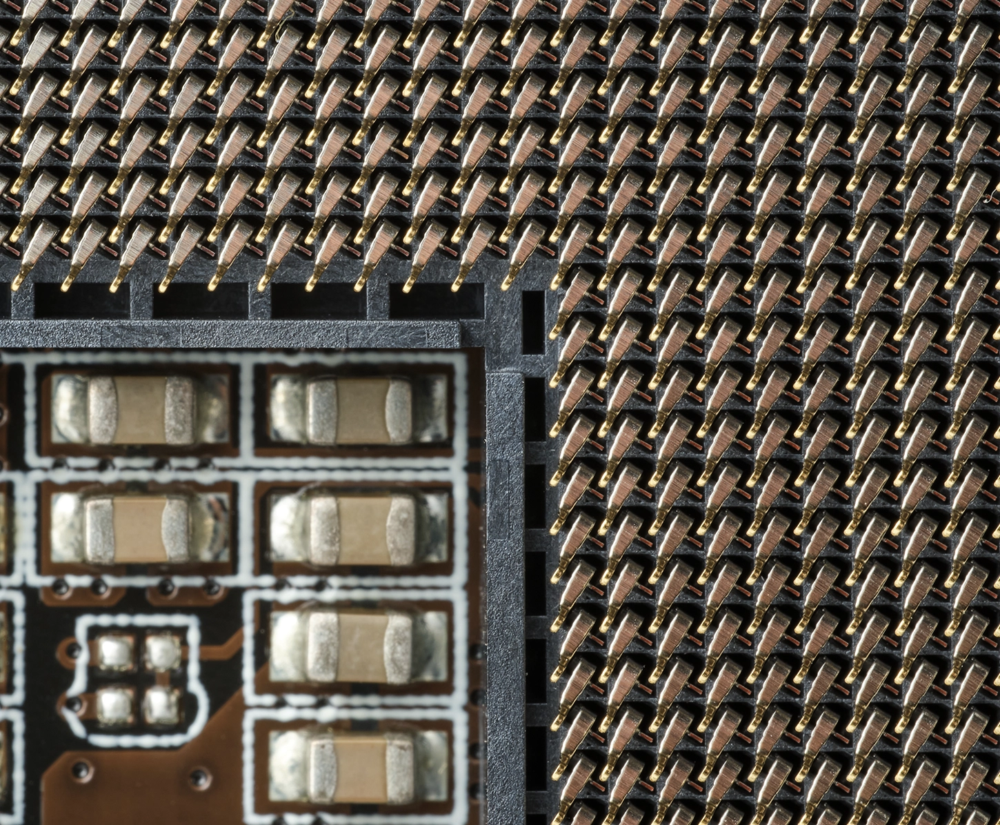
Lead frames play a critical role in semiconductor packaging by providing electrical pathways between semiconductor dies and external circuitry. Semiconductor lead frame manufacturing requires extremely fine-pitch geometries, tight tolerances, and consistent edge quality to support high-density electronic packaging applications.
E-Fab manufactures precision etched lead frames with:
- Fine-feature precision for miniature electronic assemblies
- Burr-free edges for improved electrical reliability
- Tight dimensional consistency across production runs
- Stress-free manufacturing without distortion
- Prototype-to-production scalability
Photochemical etching is particularly well suited for semiconductor lead frames because it enables intricate conductive geometries without the tooling wear, burr formation, or dimensional drift associated with conventional stamping processes.
Etched Bus Bars
Etched bus bars are used throughout semiconductor power systems, power modules, and advanced electronics applications where conductivity, thermal performance, and dimensional precision are critical.
E-Fab manufactures etched copper bus bars and conductive metal components using thin-gauge copper, phosphor bronze, and specialty conductive alloys engineered for demanding electrical applications.
Benefits of photochemical etching for bus bars include:
- Precision thin-metal processing
- Burr-free conductive edges
- Tight tolerance control
- Complex geometries without distortion
- Improved consistency versus stamped bus bars
- Reduced secondary finishing requirements
Copper and phosphor bronze materials are commonly selected for semiconductor bus bar applications because of their conductivity, thermal performance, and manufacturability characteristics.
Bipolar Plates
Bipolar plates are used in fuel cells, energy systems, and semiconductor-related thermal management applications where flow channel precision and corrosion resistance are essential.
E-Fab manufactures precision fuel cell bipolar plates and etched flow-field components capable of maintaining consistent channel geometries and repeatable production quality.
Photochemical etching enables:
- Fine-feature flow channel geometries
- Precision thin-metal processing
- Repeatable dimensional accuracy
- Burr-free manufacturing
- Corrosion-resistant material compatibility
- Production scalability for fuel cell programs
For etched fuel cell plates and advanced energy applications, photochemical machining provides greater geometric flexibility and more consistent dimensional control than traditional machining or stamping methods.
RF Shielding Components
Semiconductor systems and advanced electronics applications frequently require EMI/RFI shielding components capable of protecting sensitive electronic assemblies from electromagnetic interference.
E-Fab manufactures precision RF shield cans, shield frames, and etched EMI/RFI shielding components with:
- Thin-metal precision geometries
- Tight-tolerance apertures and openings
- Repeatable dimensional consistency
- Burr-free edge quality
- Fine-feature precision for dense electronic assemblies
Engineering Challenges in Semiconductor Component Manufacturing
Semiconductor equipment engineers face increasingly demanding manufacturing constraints as components continue shrinking in size while performance requirements continue increasing. Depending on the substrate and feature requirements, engineers may also evaluate wet etching and dry etching methods alongside broader metal etch options.
Common manufacturing challenges include:
- Achieving micro-scale features with tight tolerances
- Maintaining burr-free edge quality
- Preventing dimensional variation across production volumes
- Eliminating heat-affected zones impacting conductivity
- Supporting thermal and electrical performance requirements
- Reducing secondary deburring operations
- Managing tool wear and dimensional drift in stamping
- Maintaining repeatability at the production scale
- Supporting first-pass yield (FPY) objectives exceeding 98%
Conventional manufacturing methods often struggle to maintain the dimensional consistency and fine-feature precision required for semiconductor-grade components. As a wet, chemical process, chemical baths use liquid etchants to remove material and generally etch uniformly in all directions.
Laser cutting can introduce heat-affected zones that alter material properties and impact conductivity, while stamping processes can create burrs, dimensional drift, and tooling-related inconsistencies over long production runs. By contrast, plasma etching is a form of dry etching that removes material with gases or plasmas inside a vacuum chamber for more anisotropic results and high selectivity, though it uses more complex and expensive equipment, while wet etching relies on simpler tanks or baths and generates liquid waste instead of gaseous by-products, some of which may be toxic and require treatment.
Why Photochemical Etching for Semiconductor Parts
Photochemical etching is an advanced technology for semiconductor and advanced electronics manufacturing, offering a cost-effective option for prototypes and production while producing precision metal components and complex geometries at no extra tooling cost without mechanical stress, tooling wear, or thermal distortion.
For lead frames, bus bars, and bipolar plates, stamping introduces burrs and laser cutting creates heat-affected zones. Photochemical etching is a manufacturing process, also known as chemical milling and photochemical machining, that supports flexible production and scalable output while preserving material integrity by eliminating mechanical stresses and heat-affected zones, with burr-free edges and production-scale repeatability without secondary finishing.
Benefits of the Semiconductor Photo Etching Process
- Burr-free, stress-free manufacturing
- No heat-affected zone (HAZ)
- Sub-micron pattern fidelity
- High precision in thin metals with tolerances as tight as ±0.025mm
- Complex geometries without distortion and with a 1:1 aspect ratio at no extra tooling cost
- Better suitability for ultra-thin conductive metals
- Improved dimensional repeatability
- No tooling wear impacting consistency
- Digital tooling supports fast, inexpensive revisions compared with heavy steel stamping molds, while preserving strong design capabilities
- Faster iteration during prototyping because design changes only require digital file updates, making revisions quick and cost-effective
- Prototype-to-production scalability for one-off prototypes and high-volume production
- Yield-focused manufacturing consistency
Unlike conventional fabrication methods, photo etching on metal maintains material integrity while enabling extremely fine features and intricate geometries required for semiconductor applications.
Why Semiconductor Engineers Choose Etching Over Stamping or Laser Cutting
Stamping Limitations
While stamping can support high-volume production, it introduces several limitations for semiconductor-grade components:
- Burr formation requiring secondary finishing
- Tool wear causing dimensional drift
- Limited capability for fine-feature geometries
- Material stress and distortion
- Higher tooling costs for design iterations
Laser Cutting Limitations
Laser processing can introduce thermal effects that negatively impact semiconductor component performance:
- Heat-affected zones (HAZ)
- Potential conductivity degradation
- Edge quality concerns in thin conductive metals
- Thermal distortion
- Reduced precision in ultra-thin materials
Advantages of Photochemical Etching
Photochemical etching eliminates many of the limitations associated with conventional manufacturing methods:
- Burr-free edge quality
- No HAZ or thermal distortion
- Stress-free manufacturing
- Sub-micron fidelity
- Exceptional repeatability
- Improved dimensional consistency
- Reduced secondary finishing
- Better suitability for thin conductive metals
- Consistent production scalability
For semiconductor applications requiring fine-feature precision and repeatable dimensional control, photochemical etching provides superior manufacturability compared to stamping or laser cutting.
Materials for Semiconductor Components
E-Fab supports semiconductor and advanced electronics manufacturing with photo etching on metal for sheet metal and metal sheet stock across more than 2000 metals and alloys, giving you flexible material selection for a wide range of applications.
Common semiconductor materials include:
- Copper
- Copper alloys
- Phosphor bronze
- Stainless steel
- Nickel alloys
- Titanium
- Aluminum
- Specialty conductive alloys
Common options include stainless steel, titanium, aluminum, copper, and many alloys, with a typical metal thickness range of 0.07mm to 2.5mm for photo etched parts, supporting a variety of applications and tolerances as tight as ±0.025mm.
Copper & Copper Alloys
Copper and copper alloys are commonly used for etched bus bars, conductive interconnects, and semiconductor power distribution systems because of their high electrical conductivity and thermal performance characteristics.
Phosphor Bronze
Phosphor bronze offers an excellent combination of conductivity, strength, and spring characteristics for semiconductor bus bars and conductive applications requiring dimensional stability and fatigue resistance.
Stainless Steel & Nickel Alloys for Ferric Chloride Etching
Stainless steel and nickel alloys are frequently selected for semiconductor shielding, fuel cell bipolar plates, and corrosion-resistant precision components operating in demanding environments.
Manufacturing Capabilities & Tolerances
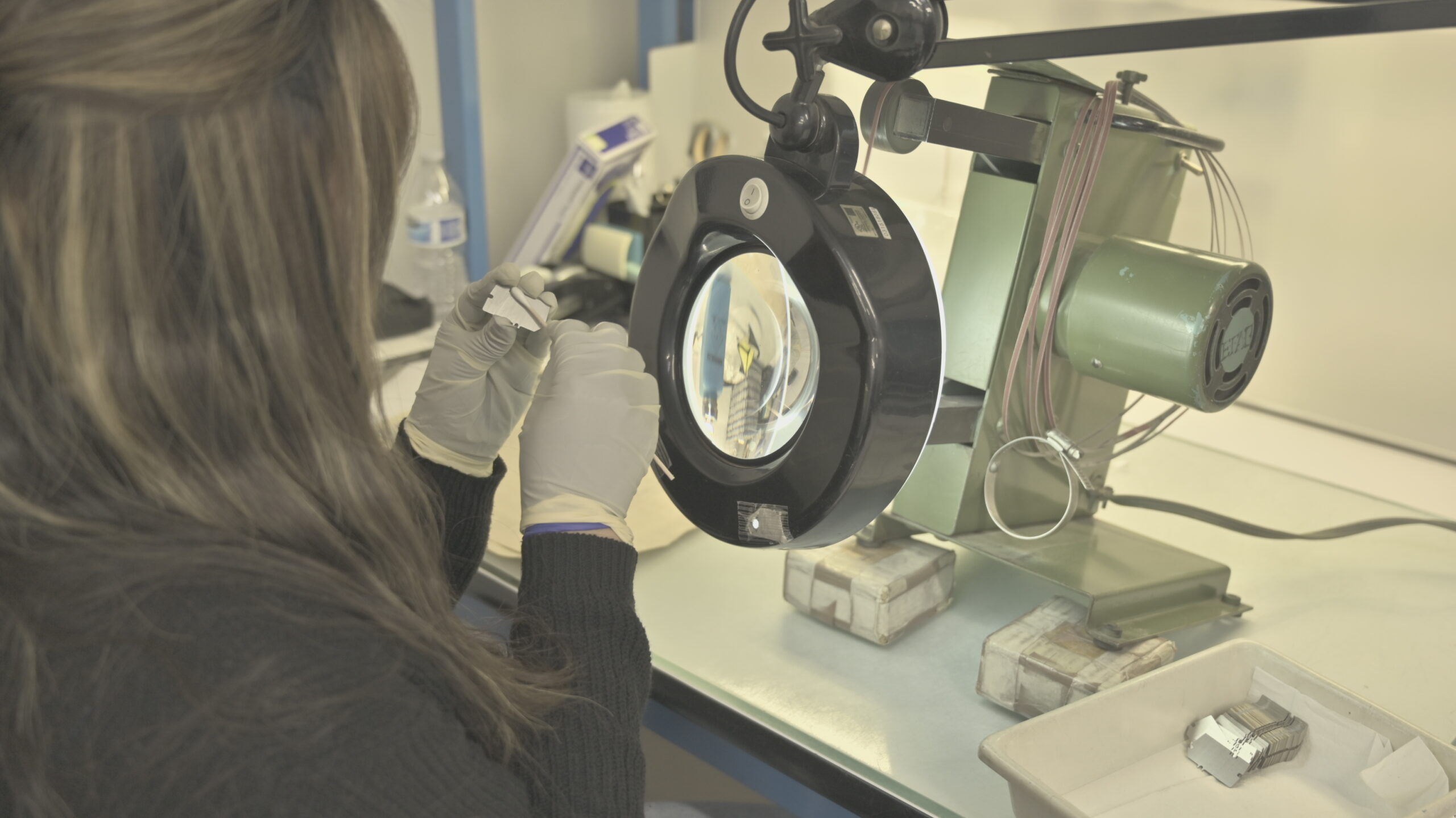
E-Fab manufactures semiconductor-grade precision etched metal components with a focus on repeatability, dimensional consistency, and yield optimization.
Capabilities include:
- Tight-tolerance photochemical etching
- Sub-micron pattern fidelity
- Fine-feature thin-metal processing
- Burr-free edge quality
- High-volume repeatability
- Prototype-to-production scalability
- Integrated forming and finishing operations
- Consistent dimensional control across production runs
Because photochemical machining does not involve hard tooling contact, E-Fab maintains repeatable dimensional accuracy without the tooling wear and drift associated with stamping operations.
This supports:
- Reduced secondary finishing
- Improved first-pass yield (FPY)
- Supplier qualification confidence
- Production-volume manufacturing consistency
Semiconductor & Advanced Electronics Applications
E-Fab manufactures etched precision parts for semiconductor and advanced electronics applications as part of photo etching work used across various industries, including:
- Semiconductor packaging systems
- Semiconductor power modules
- RF shielding systems
- Precision conductive interconnects
- Power distribution assemblies
- Fuel cell systems
- Semiconductor equipment assemblies
- EMI/RFI shielding components
- Advanced electronics manufacturing
- Microfabrication systems, with broader use in electronics, medical, aerospace, and decorative applications
How E-Fab Supports Semiconductor Applications
E-Fab partners directly with semiconductor equipment manufacturers, OEMs, and engineering teams to support manufacturability, performance optimization, and scalable production requirements.
Our semiconductor manufacturing support includes:
- Precision etching expertise for complex components
- Material selection guidance
- Prototype-to-production scalability
- Tight-tolerance process control
- Burr-free manufacturing capabilities
- Yield-focused repeatability
- Supplier qualification support
- U.S.-based production capabilities
At E-Fab, we support semiconductor reshoring initiatives and advanced electronics manufacturing growth through scalable domestic precision manufacturing capabilities aligned with evolving semiconductor supply chain requirements.
The company’s experience supporting semiconductor, RF shielding, fuel cell, and advanced electronics programs reinforces long-term production scalability and manufacturing consistency across demanding applications.
Related Capabilities & Resources
Learn more about E-Fab’s semiconductor and precision manufacturing capabilities:
Request a Quote for Semiconductor Components
When partnering with E-Fab, you can rely on our team to manufacture burr-free, precision photo-etched semiconductor components engineered for demanding applications requiring fine-feature precision, dimensional consistency, and scalable production repeatability.
Discuss your semiconductor component requirements with E-Fab’s engineering team.
Review manufacturability requirements, evaluate materials and tolerances, and identify the best process for your fine-feature semiconductor components.