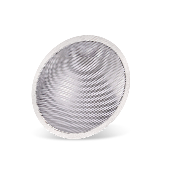
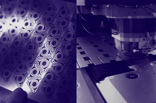
Etched Aerospace Filters & Screens: Why Precision Matters at Altitude
Explore the performance and challenges of aerospace screens in this insightful article. Discover key factors influencing their effectiveness. Read more now!
Explore the performance and challenges of aerospace screens in this insightful article. Discover key factors influencing their effectiveness. Read more now!
Explore the applications and advantages of photochemical etching and diffusion bonding. Learn how these precision manufacturing processes complement each other to achieve high-integrity components. Read more!
Discover the key differences between photochemical etching and metal stamping. Learn which process is best for precision, cost, and scalability with E-Fab’s expertise.
Discover the key differences between photochemical etching and metal stamping. Learn which process is best for precision, cost, and scalability with E-Fab’s expertise.
Discover the key differences between photochemical etching and metal stamping. Learn which process is best for precision, cost, and scalability with E-Fab’s expertise.
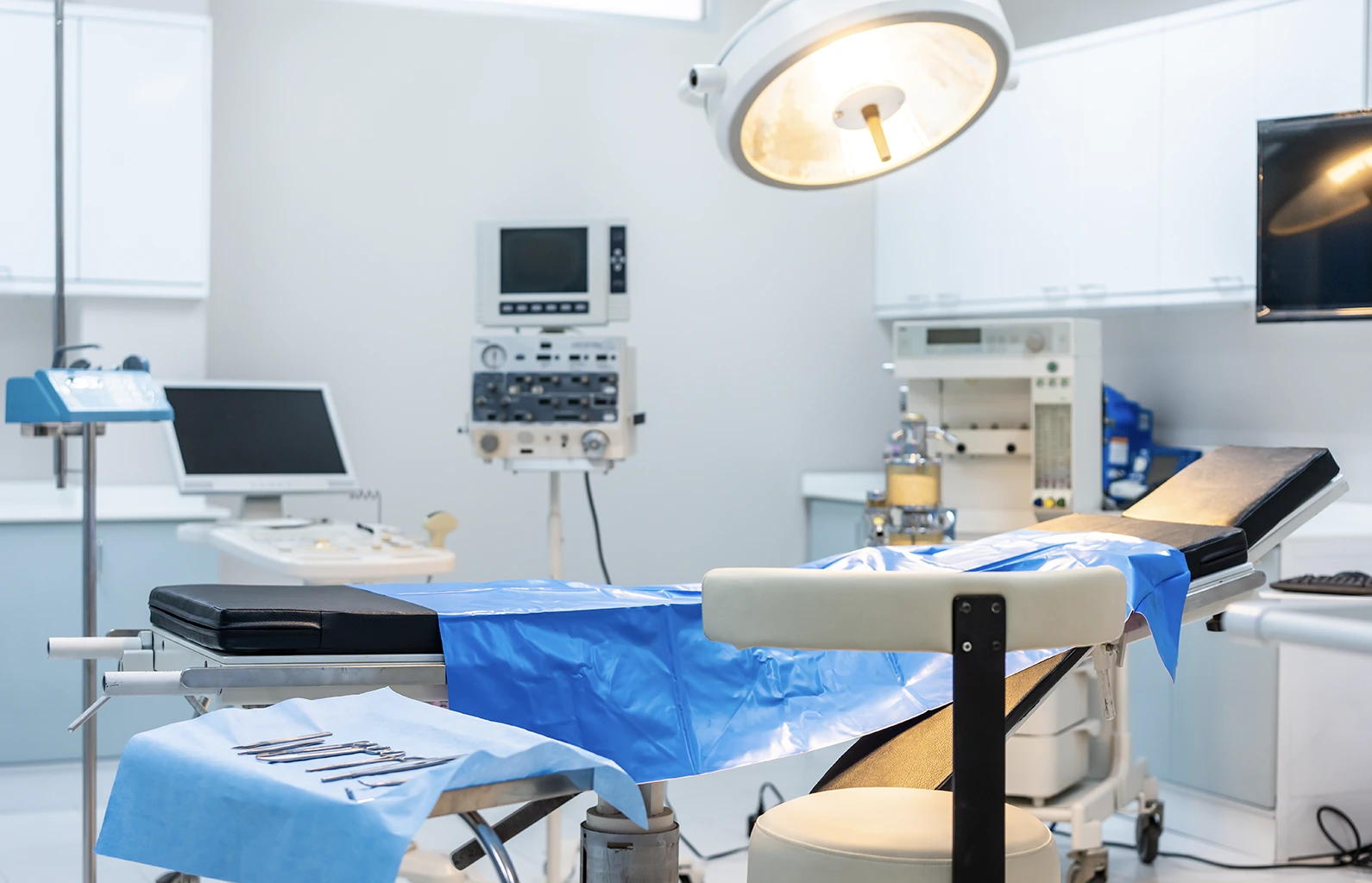
In this article, we explore PCE’s many advantages over traditional machining methods and why it’s the ideal process for crafting high-quality medical instruments.
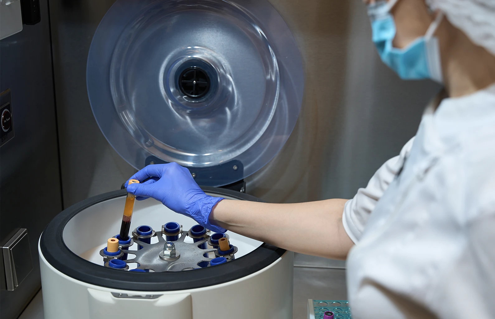
In this article, we explore the importance of precision in medical devices and the applications of precision parts in medical devices that help deliver advanced medical care.
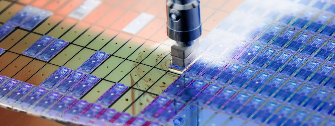
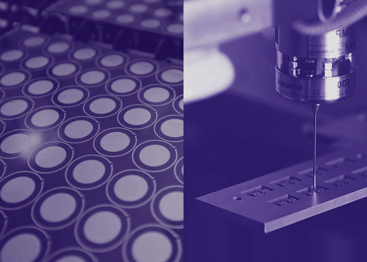
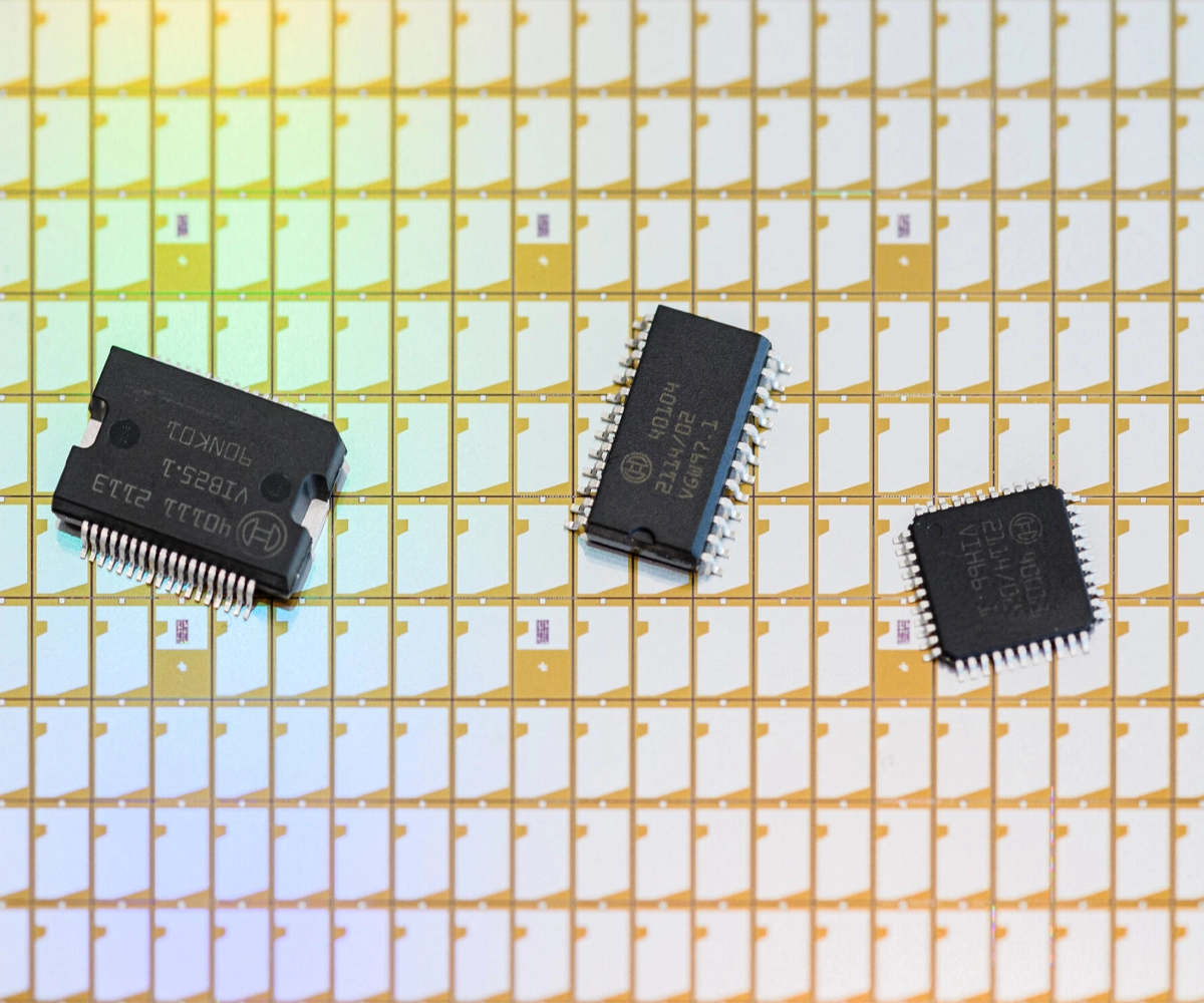
In this article, we will explore the semiconductor etching process, its key applications, advantages and importance in producing high-quality components for the industry.
In this article, we explore the photochemical etching process, its benefits, and exactly how this innovative process improves the quality of electronic components and advances the electronics industry as a whole.
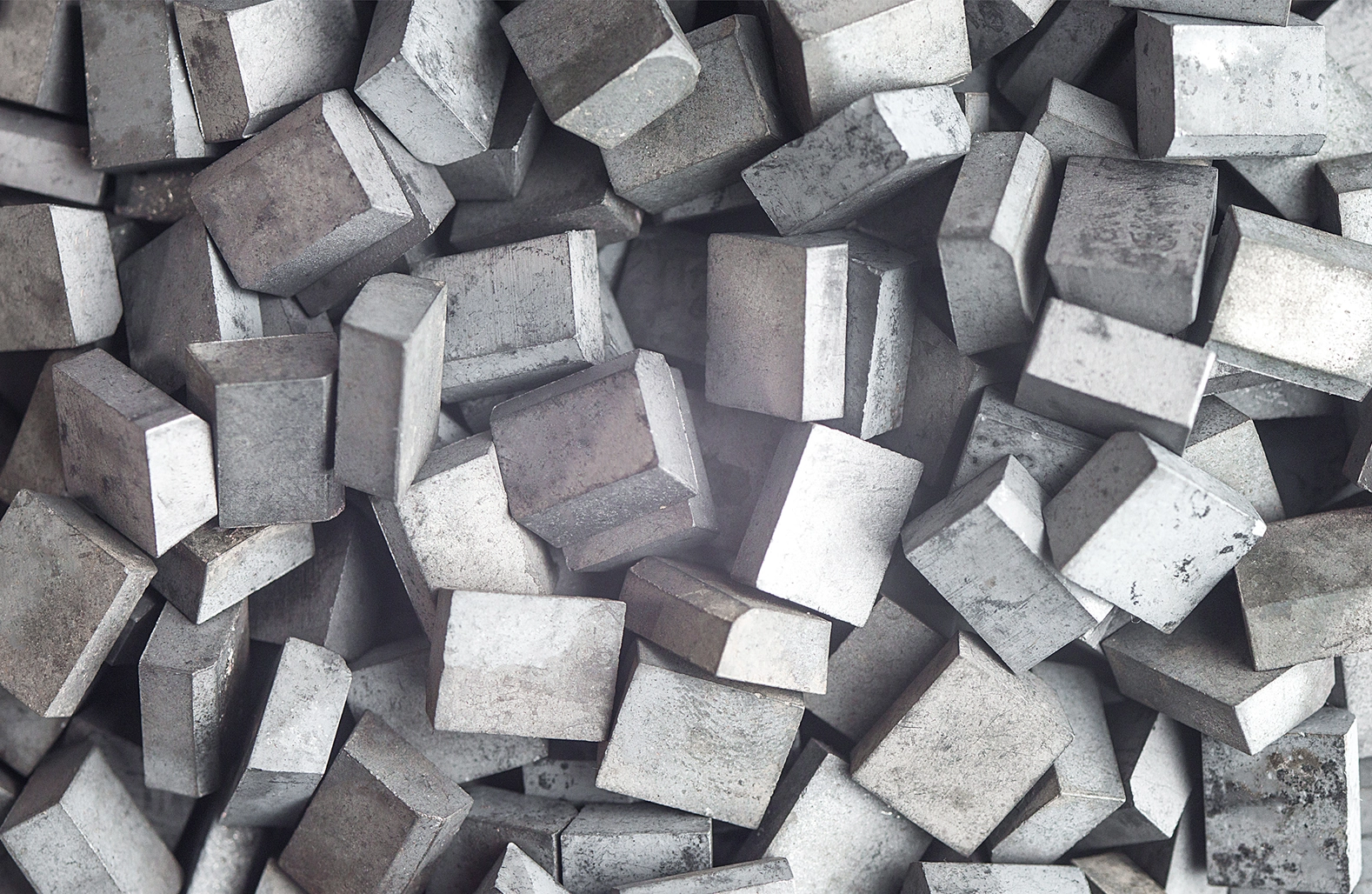
This blog article explores the common use cases for photochemically etched tungsten, highlighting its applications across different industries and the advantages it offers.