
When it comes to manufacturing precision metal parts, two advanced processes often come up in conversation: Photochemical Etching (PCE) and Diffusion Bonding. Both techniques are widely used in high-precision industries such as aerospace, medical devices, and electronics, and while they each have their strengths, they serve different functions and are suited to different stages or aspects of a component’s design and fabrication. The aerospace industry relies heavily on these processes for producing high-precision components that meet stringent performance standards.
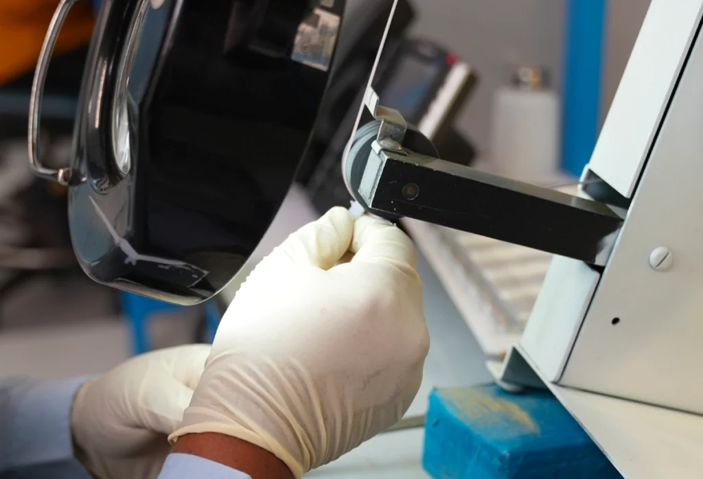
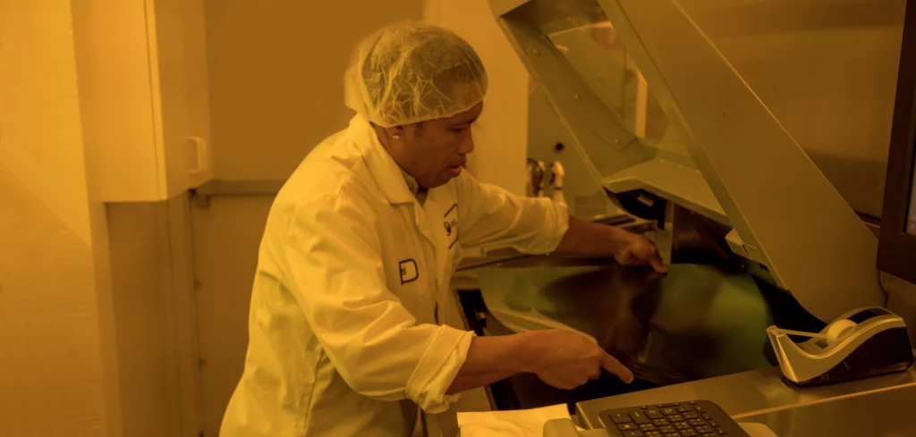
At E-Fab, photochemical etching isn’t just a capability, it’s a core specialty honed over more than four decades of hands-on experience. We’ve refined every step of the process, from phototool design and photoresist application to chemical etching and final inspection, allowing us to deliver consistently high-quality results with quick turnaround times. Components produced through photochemical etching are designed to withstand harsh environments, ensuring durability and reliability in demanding applications. Our in-house experts leverage their extensive experience to ensure high precision, superior quality, and compliance with industry standards. Our in-house engineering team works closely with clients to optimize part designs for manufacturability and post assembling and joining processes like diffusion bonding, ensuring that even the most challenging features can be realized accurately and efficiently.
Diffusion Bonding, on the other hand, is used to fuse multiple metal layers together at the atomic level. While it excels at creating strong, hermetic seals in multilayer assemblies and is often used in conjunction with photochemical etching to build complex, three-dimensional structures, it does not offer the same flexibility in shaping or patterning individual layers.
To ensure optimal manufacturability, it’s best to involve E-Fab’s engineers early in the design process. Our team can evaluate component designs for PCE feasibility, ensuring the etched features align with production capabilities. Additionally, we collaborate closely with diffusion bonding specialists to confirm alignment holes are correct and that any necessary features for successful bonding are incorporated.
By partnering with E-Fab from the outset, you can streamline development, optimize component precision, and achieve high-performance results in aerospace and other high-precision applications.
This article explores the strengths of both Photochemical Etching (PCE) and Diffusion Bonding, helping engineers and designers determine the best approach for their specific applications. PCE, particularly when executed by a specialized partner like E-Fab, offers unmatched precision, design complexity, and production scalability—making it an ideal solution for demanding aerospace, medical, and electronics components. Understanding how these processes complement each other ensures optimal manufacturability and performance.
What Is Diffusion Bonding?
Diffusion Bonding is a highly specialized solid-state joining process that creates exceptionally strong, high-integrity bonds between two or more metal surfaces without the need for melting or filler materials. Instead of relying on traditional welding or adhesives, this method uses a combination of elevated temperature and high pressure applied over an extended period of time. Under these conditions, the atoms at the surfaces of the metals gain enough energy to interdiffuse across the interface, effectively eliminating any boundary between the parts and forming a single, continuous metallic structure at the molecular level.
Because the metals are joined without melting, diffusion bonding preserves the original material properties, including microstructure, dimensional stability, and mechanical strength. This makes it ideal for applications where precision and material integrity, including electrical conductivity, are critical, such as in aerospace, medical devices, microelectronics, and advanced multilayer assemblies. The process is particularly effective for bonding thin metal layers with etched complex geometries, and it allows for the creation of components with internal features, sealed channels, or intricate layered designs that would be difficult or impossible to achieve through conventional methods.
Applications:
- Aerospace components
- Medical devices requiring strong, seamless joints
- Microchannel heat exchangers in high-performance systems
- Various industrial applications requiring strong, seamless joints
Benefits:
- Produces strong joints without welding or filler materials
- Ideal for multi-layered or laminated structures
- Maintains chemical purity with minimal contamination
The process requires tight surface preparation, precise control of temperature and pressure, and custom tooling. The process is also effective at maintaining material properties under extreme temperatures, making it suitable for high-performance applications.
What Is Photochemical Etching?
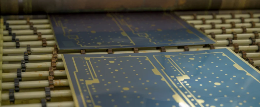
Photochemical Etching (PCE), also known as photochemical machining or chemical milling, is a precise and versatile subtractive manufacturing process used to produce intricate metal components with exceptional accuracy and repeatability. The photo etching process begins with a flat metal sheet that is thoroughly cleaned and then coated with a light-sensitive photoresist. Our team digitally image the desired pattern onto the photoresist-coated substrate using solid-state UV LEDs. The unexposed resist is removed, leaving just the mask pattern.
This processing method allows for the efficient creation of intricate components and metal parts with high precision.
Once the patterned photoresist is in place, the coated sheet is sprayed with chemical etchant, which dissolves only the unprotected areas of the metal. This results in the precise removal of material to create the final part shape while the protected areas remain intact. After etching, the remaining photoresist is stripped away, leaving behind a clean, detailed metal component.
PCE is particularly well-suited for producing thin, flat, burr-free parts with complex geometries, fine features, and tight tolerances, all without inducing mechanical stress or altering the material’s properties. It offers significant advantages over traditional machining methods, including lower tooling costs, rapid prototyping capability, and scalability for both low- and mid-volume production while being able to produce sharp edges. Industries such as aerospace, medical, electronics, and precision engineering rely on photochemical etching for parts like cooling plates, filters, meshes, shields, connectors, and multilayer assemblies, where accuracy, design freedom, and material integrity are paramount.
Applications:
- Microelectronic components
- EMI/RFI shielding
- Fine screens, meshes, and filters
- Multi-layer precision parts in aerospace, medical, and telecom
- Heat exchanger/cooling plates
- Heat sinks
- High-performance components in the electronics industry
Benefits:
- No mechanical or thermal stress on the material
- Depending on the material, thickness and features, PCE can meet tolerances as tight as ±0.0005”
- Low-cost, rapid tooling for prototyping and small-to-medium production runs
- Supports complex, intricate designs and thin materials
Additionally, photochemical etching allows for the production of precision metal components cost-effectively, making it a viable option for various applications.
When to Choose Photochemical Etching
Photochemical Etching (PCE) is the go-to solution for applications that demand thin, intricate parts with complex profiles, offering exceptional precision and the ability to achieve tight tolerances with high repeatability.
The primary benefit of photochemical etching is its ability to produce highly precise components that are challenging to fabricate with traditional methods. It’s particularly well-suited for projects requiring quick turnaround times, whether for rapid prototyping or full-scale production.
PCE excels in the fabrication of thin layers that get stacked and diffusion bonded to form multilayer parts and microstructures, making it ideal for advanced designs that traditional manufacturing methods struggle to achieve.
In addition to its technical advantages, PCE provides a cost-effective option for short to medium-production volumes, considering metal thickness, reducing tooling costs, and minimizing lead times. Its unique combination of flexibility, scalability, and precision makes photochemical etching an ideal choice for industries such as aerospace, medical, and electronics, where there’s no room for compromise on design complexity or performance.
E-Fab, Your Trusted PCE Partner
At E-Fab, we’ve built our reputation on solving the toughest challenges in metal part manufacturing, consistently pushing the boundaries of what’s possible through innovation, precision, and collaboration.
With over 40 years of industry-leading experience in precision photochemical etching, we offer unmatched expertise in producing intricate metal components with tight tolerances and superior consistency. Our capabilities extend beyond single-layer parts — we specialize in complex multilayer assemblies that integrate etching with advanced secondary bonding processes, enabling us to meet the evolving needs of next-generation applications.
Our work is trusted by engineers and manufacturers across high-stakes industries such as aerospace, medical, and electronics, where quality, reliability, and performance are non-negotiable. From mission-critical aerospace components to life-saving medical devices and high-density electronic assemblies, our solutions support some of the world’s most demanding environments.
Our advanced processes allow us to consistently produce finer geometries with greater precision than industry standards. What sets us apart is our commitment to partnership. We work closely with our customers from concept through production, offering collaborative engineering support to refine designs for optimal manufacturability, performance, and cost-efficiency.
Whether in the early stages of prototype development or scaling up for full production, E-Fab provides the precision, flexibility, and technical insight needed to bring your vision to life. Our team is passionate about solving complex problems and delivering tailored solutions that exceed expectations. When you choose E-Fab, you’re not just getting a manufacturer—you’re gaining a dedicated partner committed to your success.
Collaboration Leads to Innovation
The components produced through photochemical etching are known for their high quality and precision, meeting the stringent requirements of various industries. Backed by over 40 years of specialized expertise, E-Fab is a trusted leader in this process, delivering intricate, high-performance components for critical applications across aerospace, medical, and electronics industries.
If you’re facing a design or manufacturing challenge or simply looking for a more efficient way to produce high-precision parts, our team is here to help.