PHOTOCHEMICAL ETCHING VS ELECTROFORMING: A COMPREHENSIVE COMPARISON
In the world of precision manufacturing, both Photochemical Etching (PCE) and Electroforming are renowned for their ability to produce intricate metal components with high accuracy. However, when it comes to factors such as design flexibility, cost-effectiveness, and precision, PCE often stands out as the superior choice. Additionally, PCE offers numerous advantages that make it an ideal solution for various manufacturing needs.
E-Fab has established itself as a leader in photochemical etching, leveraging decades of expertise to deliver exceptional results in producing intricate and high-precision metal components. Our in-depth understanding of the PCE process allows us to cater to a wide range of industries, including aerospace, electronics, and medical devices.
Within this series, we delve into the key differences, advantages, limitations, and ideal applications of these two techniques. By examining these aspects, engineers and designers will gain a comprehensive understanding of which process is best suited for their specific applications and how E-Fab’s expertise can help achieve superior outcomes through PCE.
Understanding Photochemical Etching (PCE)
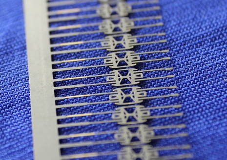
Photochemical Etching (PCE), also known as photochemical milling or photochemical machining (PCM), is a precise and cost-effective subtractive manufacturing process for producing intricate metal components with fine details and tight tolerances. Unlike conventional machining, which relies on mechanical cutting or thermal methods, PCE employs photoresist technology and chemical etchants to selectively remove material. This approach allows for the creation of complex patterns without inducing mechanical stress, distortion, or burr formation.
The PCE process involves five key steps. It begins with metal preparation, where the metal sheet is thoroughly cleaned to ensure optimal adhesion of the photoresist. Aluminum is one of the materials that can be intricately shaped through PCE. Next is the photoresist application, where a light-sensitive photoresist is uniformly applied to both sides of the sheet, serving as a protective layer. During UV exposure and image development, a photomask is placed over the coated sheet and exposed to ultraviolet light. The exposed areas of the photoresist harden, while the unexposed sections are chemically removed to reveal the bare metal. In the chemical etching stage, controlled etchants dissolve the exposed metal, forming the desired pattern. Finally, in the stripping and cleaning phase, the remaining photoresist is removed, resulting in a clean, corrosion-free component with high precision. This streamlined process facilitates the production of highly detailed and accurate metal parts without the limitations of traditional methods.
Understanding Electroforming
Electroforming is an advanced additive manufacturing process that leverages electroplating techniques to create precise and intricate metal components. The process begins with a conductive mold or mandrel, which acts as the foundation onto which metal ions are deposited from an electrolyte solution. Optimizing current density during the electroforming process is crucial for achieving lower stress values and improving the overall quality of the deposit. By applying an electric current, the metal ions are attracted to the surface of the mandrel, gradually building up in thin, uniform layers.
Electroforming is commonly used in industries such as aerospace, electronics, and medical device manufacturing. It is ideal for producing micro-scale components, precision molds, and high-fidelity replicas. Materials like nickel, copper, gold, and silver are often employed due to their strong conductivity and mechanical properties.
Key Benefits of Photochemical Etching vs. Electroforming
Photochemical etching is commonly used for precision cutting and etching of intricate patterns and features, offering the advantage of no mechanical stress or heat, making it ideal for fine detail work and prototyping. In contrast, electroforming focuses on building up metal layers to create strong, durable parts with customizable thickness, making it well-suited for applications such as mold creation, reproducing fine details, and producing parts that require high strength. Electroforming can also be used to apply coatings that enhance surface properties.
In essence, photochemical etching is often more suitable for precise, detailed patterns, while electroforming is typically chosen when strength, durability, and material buildup through plating are essential.
Precision and Detail
PCE: Offers high precision and the ability to create intricate patterns with micron-level accuracy, ideal for detailed etching work.
Electroforming: Primarily used for building up metal layers and producing strong parts but may not achieve the same level of fine detail as photochemical etching. While it can be highly precise, the process may require longer production times for components with more complicated designs.
Tool Wear and Wear Resistance
PCE: No tool wear is involved because it doesn’t rely on physical tools like cutting or stamping. This leads to lower maintenance costs and faster production.
Electroforming: Involves the use of tools or molds, which can experience wear over time and may need replacement, potentially increasing long-term costs.
Materials and Material Handling
PCE: Highly versatile and can be used with a wide range of metals and alloys without affecting their original properties.
Electroforming: Works well for creating durable parts, but its effectiveness may be limited by the type of metal and the need for precise control over thickness. Electroforming is often limited to copper or nickel parts.
Application Suitability
PCE: Better suited for fine-detail work, prototyping, or producing complex, small features without adding material.
Electroforming: More appropriate for creating strong, durable parts with customizable thickness or for mold creation.

Ideal Applications for PCE vs. Electroforming
When comparing PCE to Electroforming, it’s important to understand how the unique characteristics of each process influence their suitability for different applications. PCE is more efficient compared to traditional methods, making it a cost-effective choice. Each method has distinct advantages and limitations based on the materials, designs, and desired outcomes. Here’s an expanded look at ideal applications for each technique:
PCE is advantageous because it eliminates any heat-affected zone (HAZ) due to its cold-cutting technique. Additionally, high current density during the electrodeposition process can lead to increased internal stresses and defects like cracks, impacting the quality of electroformed parts. Nickel is often plated onto various metal surfaces to improve wear resistance, enhance decorative appearance, and provide corrosion protection.
In the electroforming process, the stability of the materials and testing instruments is crucial for ensuring accurate and reliable performance. Nickel’s wear resistance makes it suitable for applications requiring durability, such as molds and automotive parts.
Aerospace Components:
PCE: Precision shims, gaskets, and filters for jet engines and satellite components.
Electroforming: Waveguides and microwave filters.
Medical Devices:
PCE: Components for surgical instruments such as coblation electrodes or catheter tips, diagnostic equipment, and implantable components such as maxillofacial mesh or orthopaedic implants.
Electroforming: Catheter tips and miniature implants.
EDM: Complex surgical tools, orthopedic implants, and precision-machined medical instruments.
Electronics & Semiconductors:
PCE: EMI/RFI shielding, lead frames, and flexible circuits.
Electroforming: Microfluidic channels and precision molds for microchip production.
Automotive:
PCE: Fuel injector components, fine mesh filters, heat exchangers, and sensor components.
Electroforming: Fuel injector nozzles and fine mesh filters
The Manufacturing Partner You’ve Been Searching For
While both Photochemical Etching and Electroforming excel in producing precise metal components, PCE emerges as the superior option for manufacturers seeking high precision, design flexibility, and cost-effectiveness. Its ability to handle intricate designs with minimal lead time makes it ideal for industries such as aerospace, medical devices, and electronics.
On the other hand, Electroforming remains valuable but limited to niche applications requiring complex 3D structures and specialized material properties. By understanding the strengths and limitations of each method, manufacturers can make informed decisions to optimize their production processes and achieve exceptional results.
Partner with E-Fab today! We’re excited to collaborate with you in producing precision components that combine unmatched quality and innovation, all made possible through our Photochemical Etching process, which is recognized as the industry standard.