
In today’s world of increasingly compact, connected, and high-performance electronics, electromagnetic interference (EMI) is a constant threat. For example, EMI can disrupt critical equipment in medical devices, aerospace electronics, transit systems, and navigation, making effective shielding essential in these real-world scenarios. From medical devices to aerospace systems and consumer IoT products, effective RF shielding often determines whether a device passes compliance or fails in the field
Effective electromagnetic shielding isn’t just about slapping a metal can over a PCB at the end of development; it’s about engineering foresight. Shielding design decisions made early in the process have a direct impact on product performance, reliability, manufacturability, and cost. This applies to various types of equipment, including audio speakers with metallic casings, rack-mounted servers, and other devices that require protection from EMI to ensure signal integrity.
This guide covers essential shielding design considerations, from enclosure and PCB strategies to material selection and manufacturing and shows how partnering with a precision manufacturer like E-Fab can help you avoid costly redesigns and accelerate time-to-market. It is important to consider shielding for various types of electronic equipment and other devices early in the design process to ensure proper operation and minimize interference.
The Importance of Early RF Shielding Design
One of the most common mistakes in EMI mitigation is treating rf shielding as an afterthought. Attempting to retrofit shielding late in the design cycle often leads to:
- Increased part count, weight, and cost
- Larger enclosures or redesigns to accommodate shielding features
- Missed regulatory deadlines due to compliance failures
- Difficulties in retrofitting shielding for cables and cable access points, which can become major sources of electromagnetic interference if not properly addressed
Early-stage consideration of shielding design ensures your device not only meets EMI/RFI standards but also remains manufacturable and optimized for performance. By planning shielding strategies early, including proper cable entry and access point protection, you can integrate solutions seamlessly, reduce risk, and improve reliability.
Enclosure Design Best Practices
A well-designed enclosure is your first line of defense against EMI. Enclosures may use sheet metal, foil, or conductive composites, including plastics filled with conductive particles, to balance performance, weight, and cost. It acts as a Faraday cage, blocking unwanted signals from entering or escaping. Here’s how to maximize its effectiveness:
Seam Placement and Gasketing
Every seam is a potential EMI leakage path. Position seams away from high-emission zones and ensure tight, continuous contact between mating surfaces. Conductive gaskets, often made from metal-filled silicones or spring contacts, maintain shielding effectiveness while allowing repeated assembly and disassembly. Some EMI gaskets also include an inner layer of conductive fabric or material to enhance durability and conductivity, preventing brittleness and improving long-term performance.
Slot and Aperture Minimization
Openings, such as for connectors, displays, or ventilation, can act as antennas if not properly managed. Keep apertures as small and few as possible and use honeycomb vents or conductive mesh where airflow is required.
Layered Shielding and Partitioning
For devices with multiple high-frequency components, consider internal partitions constructed in the form of metallic foils, meshes, or other shielding materials, or use multi-layer shielding to isolate noise sources. This modular approach can significantly reduce cross-coupling and simplify EMI debugging.
Integration of Vents, Filters, and Connectors
Vents and connectors are common EMI entry points. Filtered connectors and shielded cable interfaces often incorporate a metallic casing to prevent EMI leakage. Use filtered connectors, shielded cable interfaces, and EMI-rated ventilation panels to maintain performance without compromising functionality.
PCB Design Considerations
Even the best enclosure won’t compensate for a noisy PCB layout. Good board-level design practices are essential to minimizing EMI emissions and susceptibility. Shielding electronic components on the PCB is crucial to prevent EMI emissions and protect sensitive circuits from external interference.
Trace Routing and Grounding
Keep high-frequency traces short and avoid right-angle bends. Implement a solid, continuous ground plane to provide a low-impedance return path and minimize loop area, which helps reduce magnetic field emissions. Careful trace routing and grounding control both electric and magnetic field emissions.
Component Placement
Separate noisy and sensitive components. Place high-speed devices away from analog circuitry and near their associated connectors to minimize radiating loop size.
Via Stitching
Use via stitching around the perimeter of sensitive regions or along the edges of ground planes to reduce slot radiation and improve shielding effectiveness.
Board-Level Shielding Cans
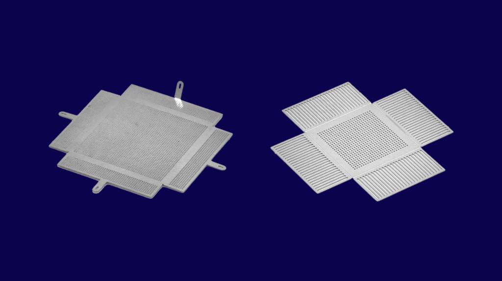
Integrate shielding cans directly on the PCB to isolate specific components or functional blocks. Shielding cans can also take the form of an inner metallic casing or be constructed from metal foams for lightweight applications. These shields, often produced with photochemical machining, can be precisely tailored to your board geometry.
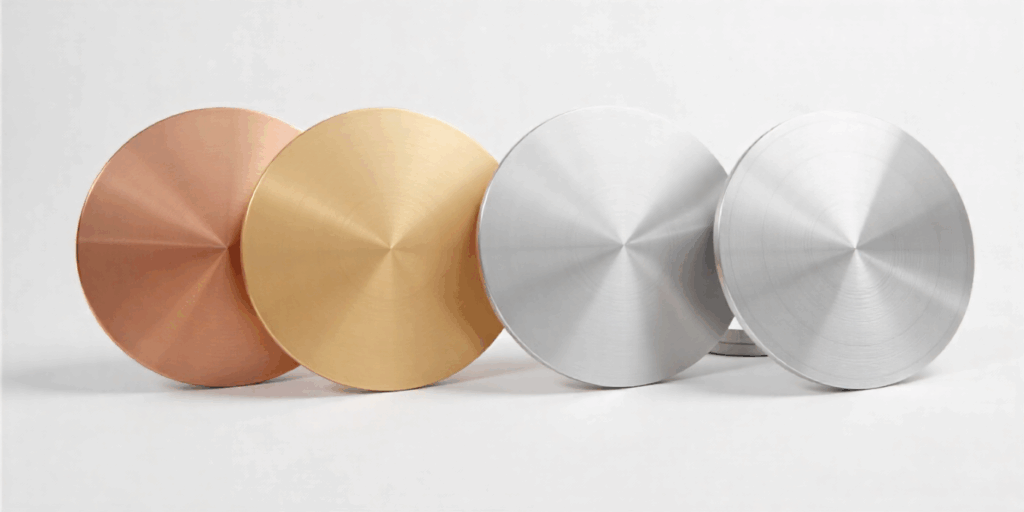
Material Selection for RF Shields
Choosing the right material is critical for balancing shielding effectiveness, mechanical strength, corrosion resistance, and cost. Common EMI shielding materials include:
- Copper: Exceptional conductivity and shielding performance, but softer and more expensive.
- Brass: Good conductivity and strength balance, often used in commercial applications.
- Nickel Silver: Excellent corrosion resistance and good mechanical properties.
- Stainless Steel: Strong and durable with moderate conductivity, ideal for rugged environments.
Other options include metal foams, conductive inks, and magnetic materials, each offering unique benefits for specific applications.
Selecting a suitable metal, such as copper, nickel, or stainless steel, is essential for effective EM shielding, especially when considering the frequency range, environmental conditions, and the specific requirements of the electronic equipment or electronic goods being protected.
Advanced EMI materials, such as metal foams and metallic inks loaded with very small particulates or small particulates of copper or nickel, are increasingly used in plastic enclosures and electronic goods. These materials provide lightweight, flexible, and effective EMI shielding, especially for devices operating at high frequencies and exposed to radio frequency or radio waves.
Conductive and magnetic materials are especially important for blocking or absorbing high-frequency electromagnetic radiation.
EMI materials are widely used to protect electronic equipment and electronic goods from electromagnetic interference, ensuring reliable operation and preventing data transmission issues.
Advances in technology, including new material formulations and innovative manufacturing processes, are enabling more effective EMI shielding solutions for modern electronic applications.
For enhanced performance, consider surface plating such as tin (for solderability), silver (for superior conductivity), or nickel (for corrosion protection). Specialty alloys may be required for harsh environments, weight-sensitive designs, or specific frequency challenges.
Shielding Effectiveness: What Really Matters
Shielding effectiveness is the cornerstone of any successful EMI shielding solution. It measures how well an EMI shield can reduce the strength of electromagnetic fields within a protected space, ensuring that sensitive electronic devices are safeguarded from unwanted electromagnetic interference (EMI) and electromagnetic radiation.
The performance of an EMI shielding material is influenced by several critical factors. The type of material, whether copper, aluminum, steel, or specialized alloys, directly impacts how much electromagnetic energy is blocked or attenuated. For example, copper is renowned for its high electrical conductivity and excels at shielding high-frequency electromagnetic waves and radio frequencies, making it a popular choice for many electronic devices. In contrast, materials like steel or mu-metal, with high magnetic permeability, are better suited for shielding against low-frequency electromagnetic fields, which are common in certain industrial and aerospace applications.
Material thickness and the size of the shielded volume also play a significant role. Thicker materials generally provide greater attenuation, but this must be balanced against weight and space constraints, especially in compact or weight-sensitive designs. Shielding performance also varies across frequencies, so selecting materials suited to your device’s operating range is essential.
The design of the enclosure or shield is equally important. Even the best EMI shielding material can be compromised by poorly designed apertures, seams, or openings. Small holes or slots may allow high-frequency electromagnetic waves to penetrate, while larger gaps can reduce overall shielding effectiveness. Employing shielding methods such as conductive gaskets, metallic foils, or coatings with high electrical conductivity can help maintain a continuous conductive path and enhance the shield’s performance.
Selecting the right shielding method, whether it’s a solid metal enclosure, a conductive coating, or a layered approach, depends on the specific requirements of the device, including the level of EMI protection needed, environmental conditions, and cost considerations. For instance, aerospace applications may demand lightweight materials with high shielding effectiveness at radio frequencies, while commercial electronics might prioritize cost-effective coatings or metallic screens.
Ultimately, understanding shielding effectiveness and the factors that influence it enables engineers and designers to choose the most suitable EMI shielding materials and methods for their application. By carefully considering material properties, enclosure design, and the operational environment, you can ensure your devices are well-protected against electromagnetic interference, maintaining performance and compliance in even the most challenging conditions.
Manufacturing Considerations
Even the best design can fall short without the right manufacturing process. Traditional stamping or machining can struggle with fine apertures, thin walls, and intricate geometries required for modern RF shields.
That’s where photo chemical machining (PCM) stands apart:
- Precision and Complexity: Achieve fine features, tight tolerances, and complex geometries without expensive tooling.
- Material Versatility: Work with thin metals and specialty alloys while maintaining structural integrity.
- Scalable Production: Seamlessly transition from rapid prototypes to full-scale production with consistent quality.
Why Work with E-Fab
At E-Fab, we do more than manufacture RF and EMI shielding, we collaborate with engineers and designers to solve complex electromagnetic challenges before they become costly problems.
Here’s why industry leaders in aerospace, defense, medical, and electronics trust us:
- Engineering Partnership: We engage early in the design process to optimize performance, manufacturability, and cost.
- Proven Expertise: Decades of experience producing precision electromagnetic shielding components for mission-critical applications.
- End-to-End Support: From rapid prototyping to volume production, we deliver quality, repeatability, and reliability.
When you work with E-Fab, you’re not just sourcing a part, you’re gaining a dedicated engineering partner committed to your product’s success.
Design Shielding Early, Design It Right, Design It With E-Fab
RF shielding design touches every part of a device’s development, from PCB layout to enclosure construction. Addressing it early makes compliance easier, improves performance, and helps control costs.
Whether you’re building a next-generation medical sensor or a rugged defense communication system, partnering with an experienced shielding manufacturer can make all the difference.
Ready to Build Your Next Shield?
Let E-Fab help you turn your concept into a compliant, high-performance product.