Powering Modern Semiconductor Manufacturing Technology
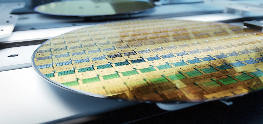
From smartphones and medical devices to automobiles and next-generation communication systems, semiconductors drive today’s innovations. At the core of these devices are precision components that must meet exacting standards to keep pace with smaller, faster, and more efficient chips.
As advanced devices increased in complexity and miniaturization, the demand for more sophisticated etching methods has grown. These intricate architectures require cutting-edge etching technologies to achieve the necessary accuracy and control.
For engineers, sourcing managers, and procurement teams, the challenge is finding a partner who can deliver components that support miniaturization, precision, and high-volume production—without sacrificing speed or cost-effectiveness.
That’s where E-Fab comes in. With decades of expertise in photochemical etching, we manufacture burr-free, stress-free, and highly repeatable components tailored to semiconductor applications.
What is Semiconductor Etching? Let's Break It Down Quickly
Etching refers to the process of removing material from a wafer or metal surface with extreme precision to create patterns, circuits, or structural features. Its primary role in manufacturing is to enable microscale features essential for modern chips, devices, and supporting components.
There are two basic mechanisms involved in etching: physical and chemical.
Physical etching – ion bombardment, sputtering
Chemical etching – chemical reactions with etchants
Most processes combine both
These basic mechanisms underpin all semiconductor etching processes, allowing for precise pattern transfer and the fabrication of high-aspect-ratio microstructures
Etching Methods: Wet Etching and More
Wet Etching
Uses chemical solutions (also known as wet chemical methods)
Characterized by its isotropic nature, meaning wet etch removes material uniformly in all directions
Simple, good for large wafer areas
Risk of undercutting → reduced pattern fidelity
Wet etch processes are often used in the initial etching steps for cleaning or large-area patterning
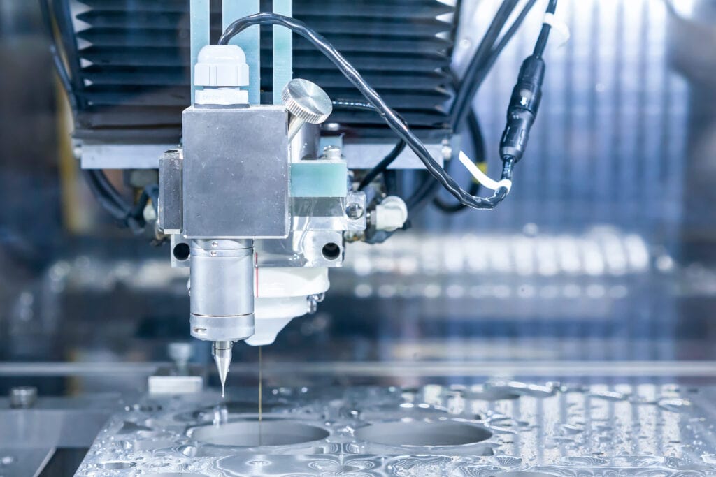
Dry etching (Plasma, RIE)
Anisotropic (directional) → high precision
Controlled by gas composition, chamber pressure, power density
Enables deep trenches, narrow vias (VLSI/ULSI)
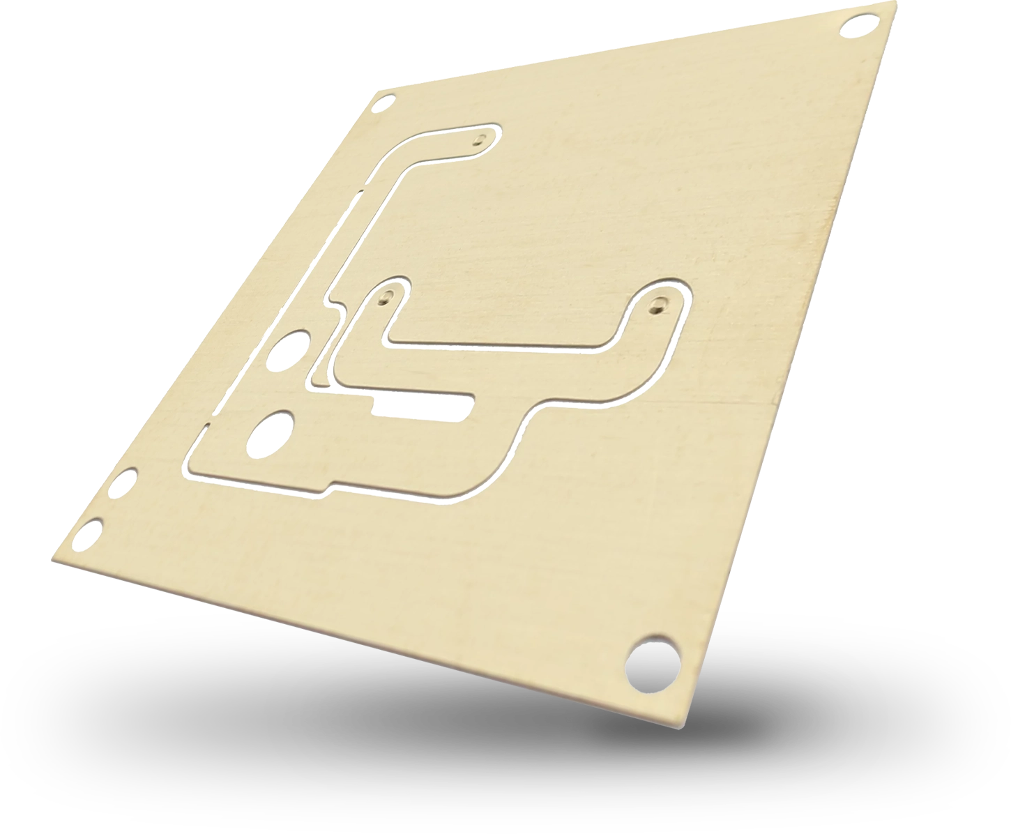
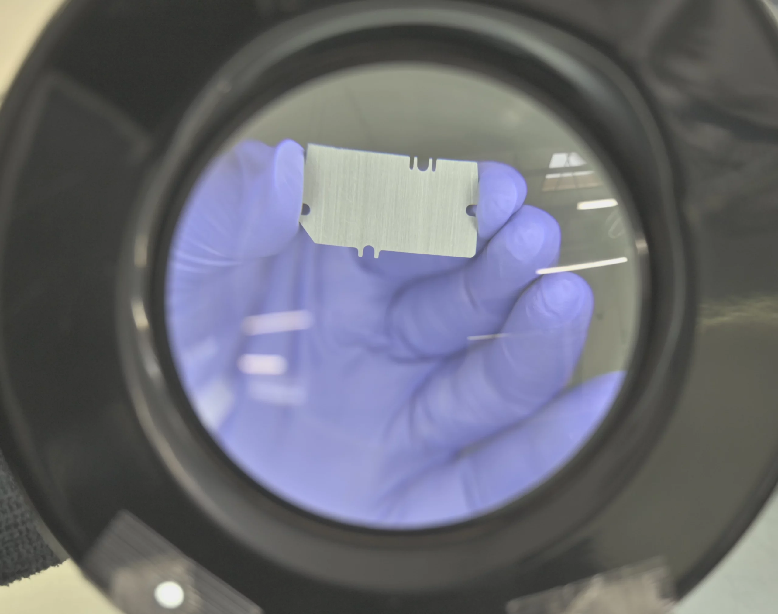
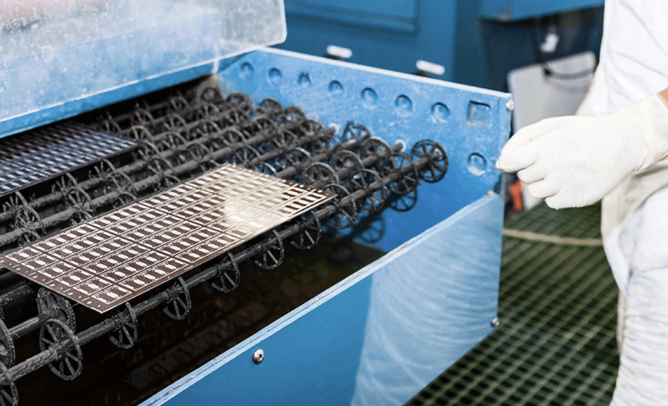
Photochemical etching/machining (E-Fab specialty)
Uses photoresist + chemical solutions on metals
Produces sharp, burr-free, stress-free thin metal components
Superior to laser cutting (avoids heat damage/slag) and stamping (avoids burrs, geometry limits)
Best suited for semiconductor precision metal parts
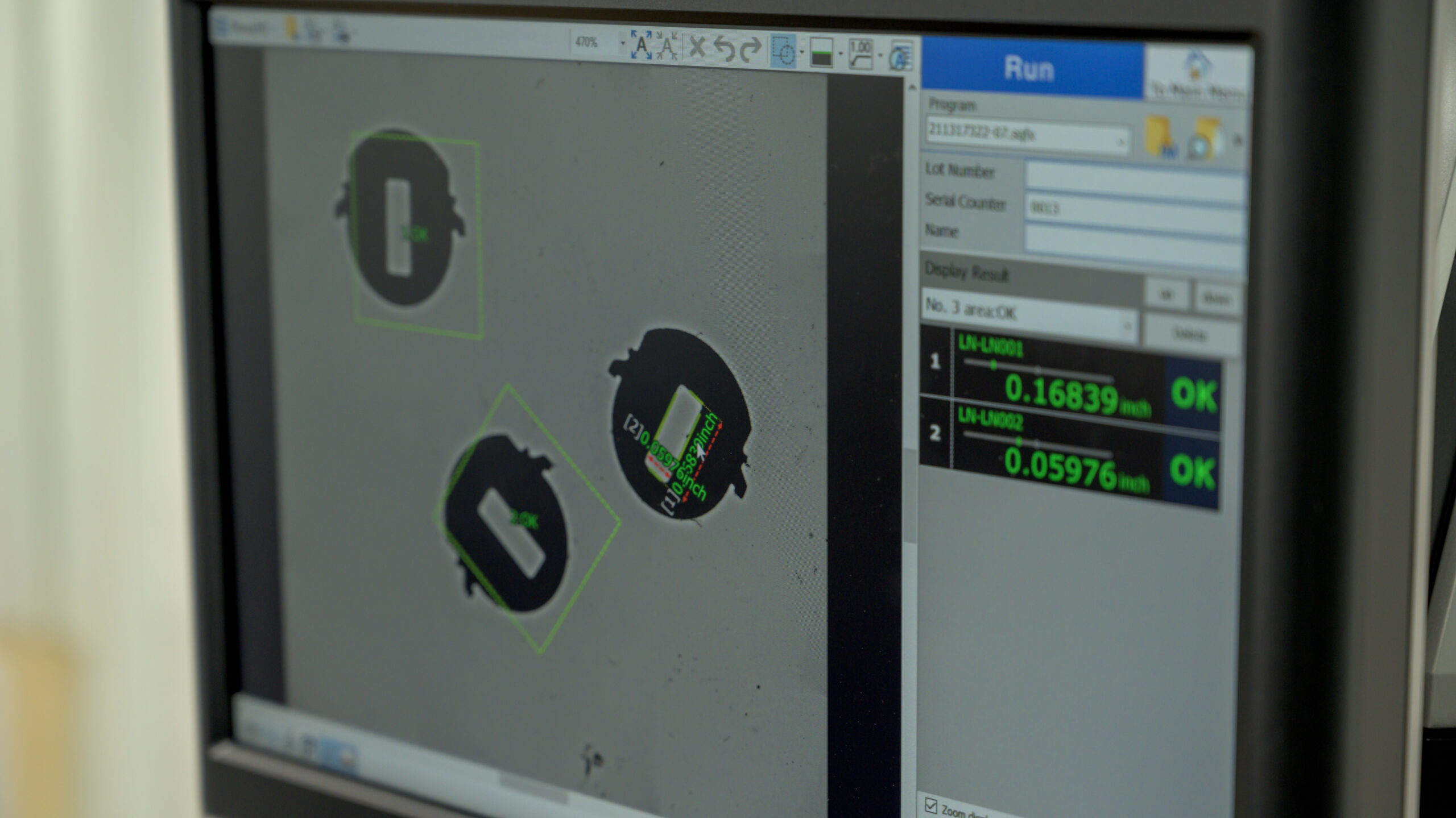
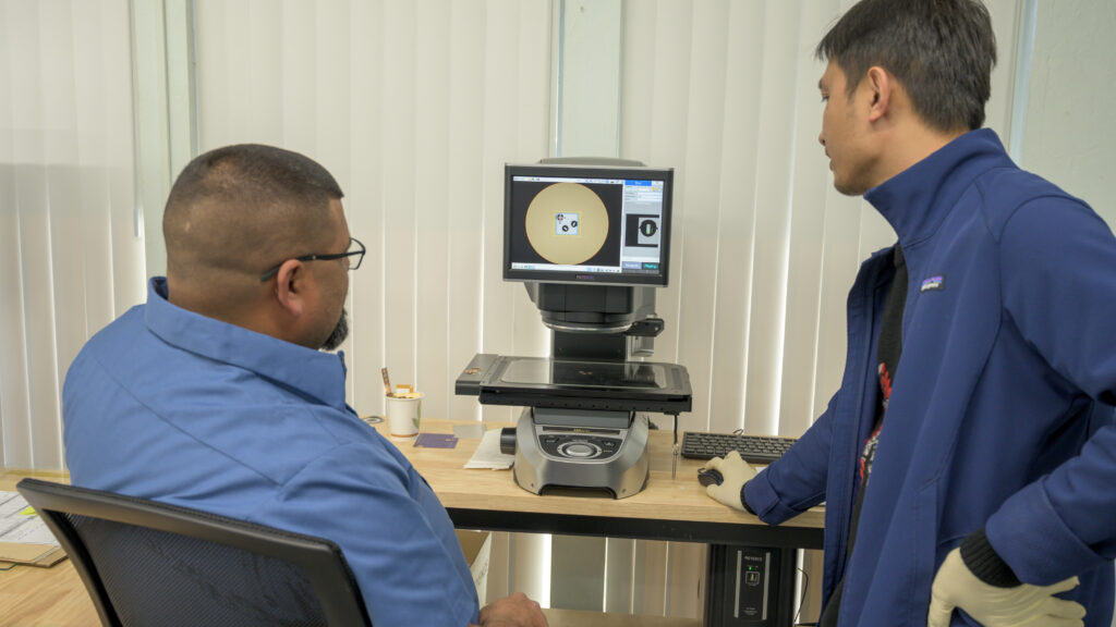
Key Process Parameters - Photochemical Etching
Etch Rate:
Determines throughput & dimensional accuracy
Controlled by material type, etchant chemistry (e.g., ferric chloride), temperature, concentration & agitation
Etch Depth & Undercut
Full-thickness etching of thin metals
PCE is an isotropic process, which means it etches laterally as well as vertically → lateral undercut must be controlled (etch time, resist adhesion and quality, solution stability)
Photoresist & Mask Quality
Accurate UV imaging and strong resist adhesion and conformity along features for multi-step etching are critical for fine features & tight tolerances
Material Properties
Alloy composition, grain structure, hardness and material thickness influence etch rate and feature tolerances
Etchant Management
To maintain product quality, etching chemistry must be maintained. Such factors include: concentration control, temperature and pH regulation, filtration to remove reaction by-products, and continuous replenishment.
Summary
Etching plays a critical role across various stages of semiconductor manufacturing, enabling the creation of high-precision micro- and nanostructures.
Etching is essential for forming structures and removing materials to create precise device features and complex geometries.
Success in semiconductor etching depends on precise control of etch rate, depth, aspect ratio, and chemistry.
Photochemical etching = ideal for burr-free, stress-free semiconductor metal components.
Benefits of Photochemical Etching for Semiconductor Components
Choosing the right etching method can directly impact semiconductor performance and reliability. With E-Fab, customers gain:
High precision and repeatability: Tight tolerances for even the most intricate designs.
Complex geometries: Capability to produce patterns that are impossible with mechanical methods.
Stress-free, burr-free components: No warping, micro-cracks, or tool-induced damage.
Cost-effectiveness: Affordable prototyping and efficient scaling for volume production.
Material versatility: Expertise across stainless steel, copper, nickel, titanium, and more, including thin film and new materials relevant to advanced semiconductor applications.
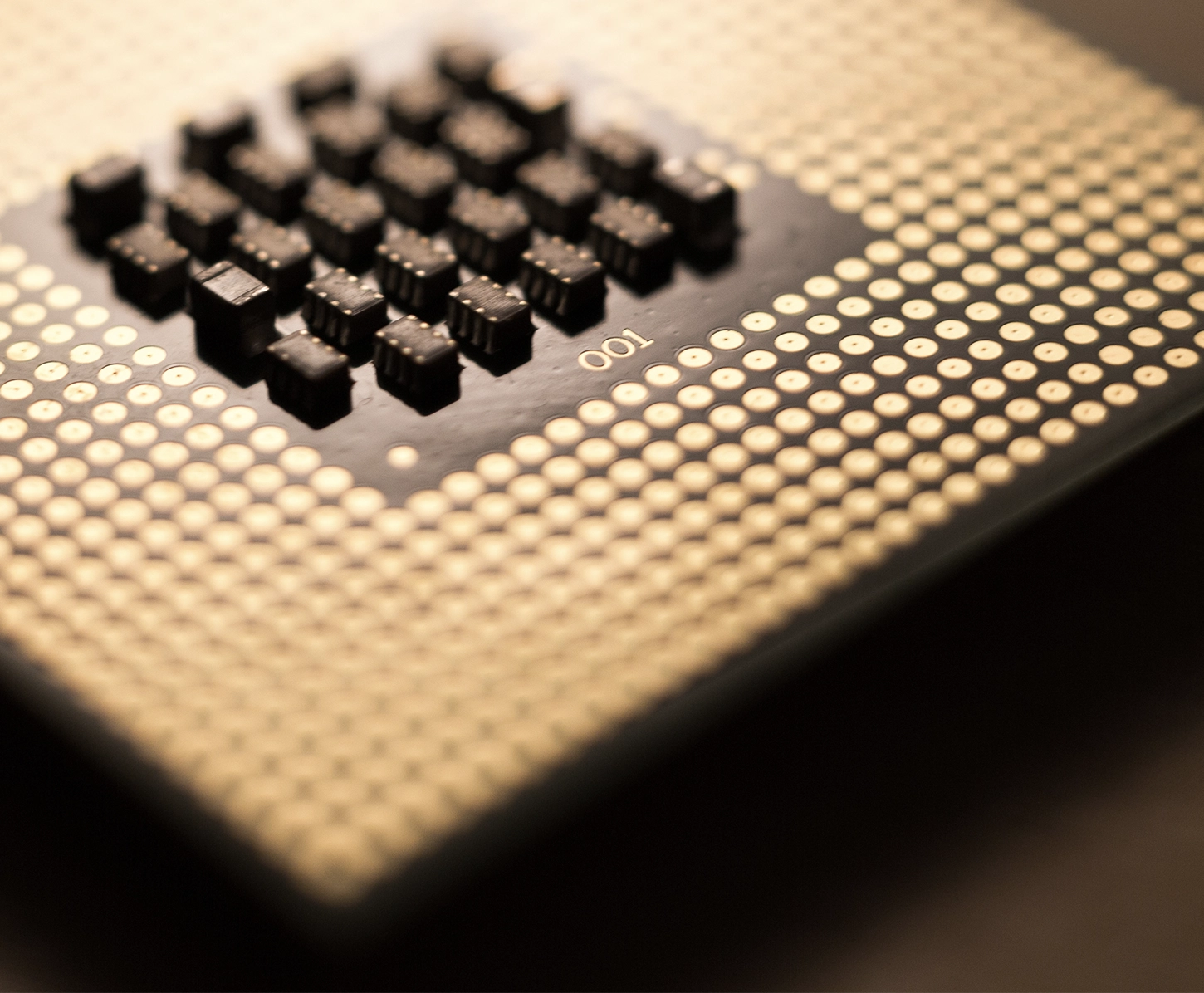
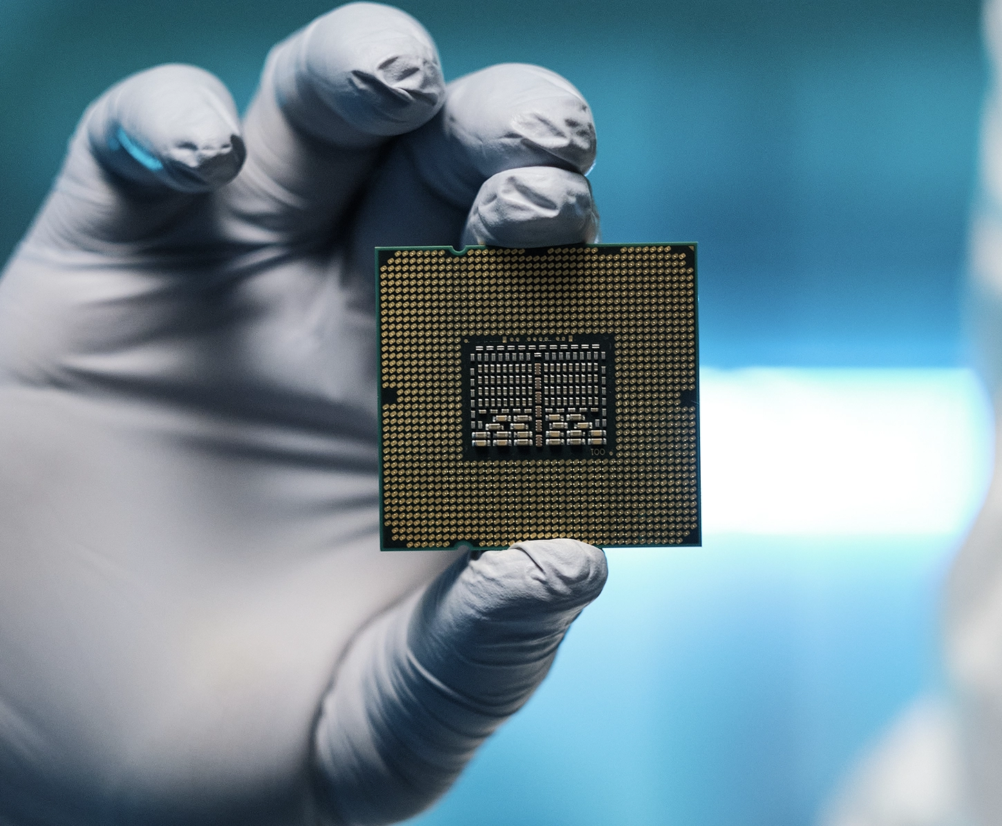
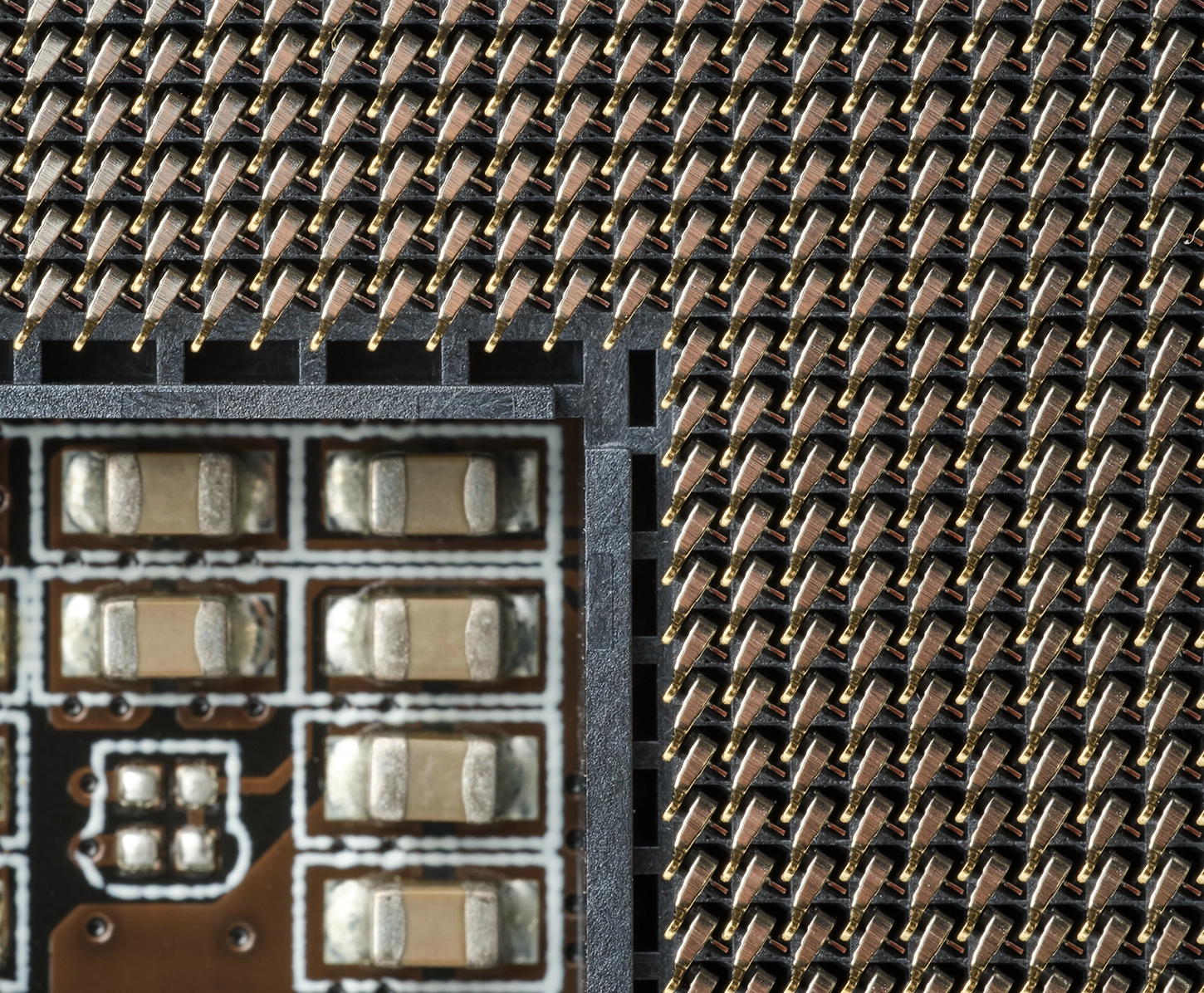
Components E-Fab Manufactures for Semiconductors
Our expertise spans across semiconductor metal fabrication for critical applications. E-Fab delivers:
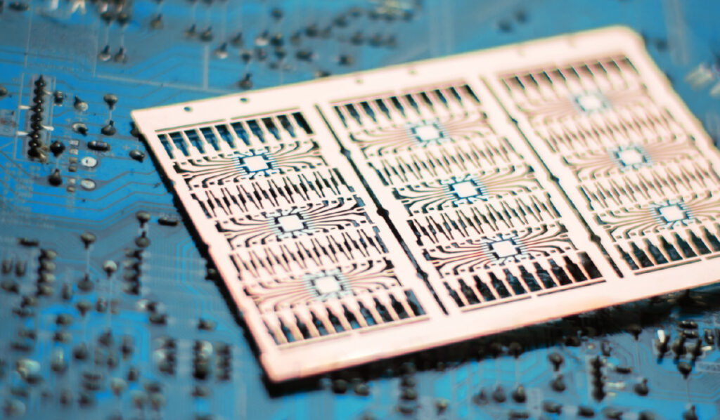
Lead frames for microelectronics, including use in wire bonding applications
Contact springs for secure electrical connections, also suitable for wire bonding processes
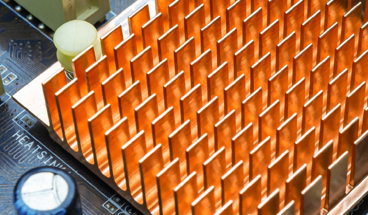
Heat sinks to manage thermal performance
EMI/RF shields for EMI/RFI protection
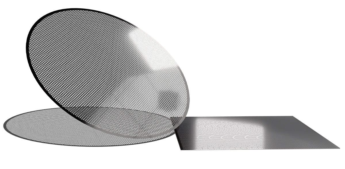
Fine meshes and filters for particle management
Custom micro-structures tailored to emerging technologies, enabling fabrication of intricate microscale components
E-Fab’s components are engineered to meet the stringent requirements of VLSI and ULSI designs, as these advanced architectures and ULSI designs demand highly precise, anisotropic etching processes for complex device fabrication.
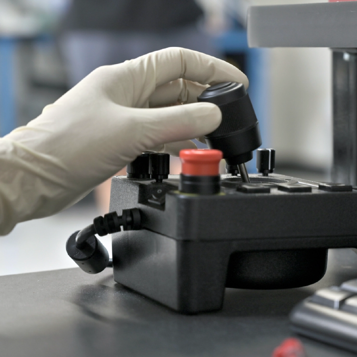
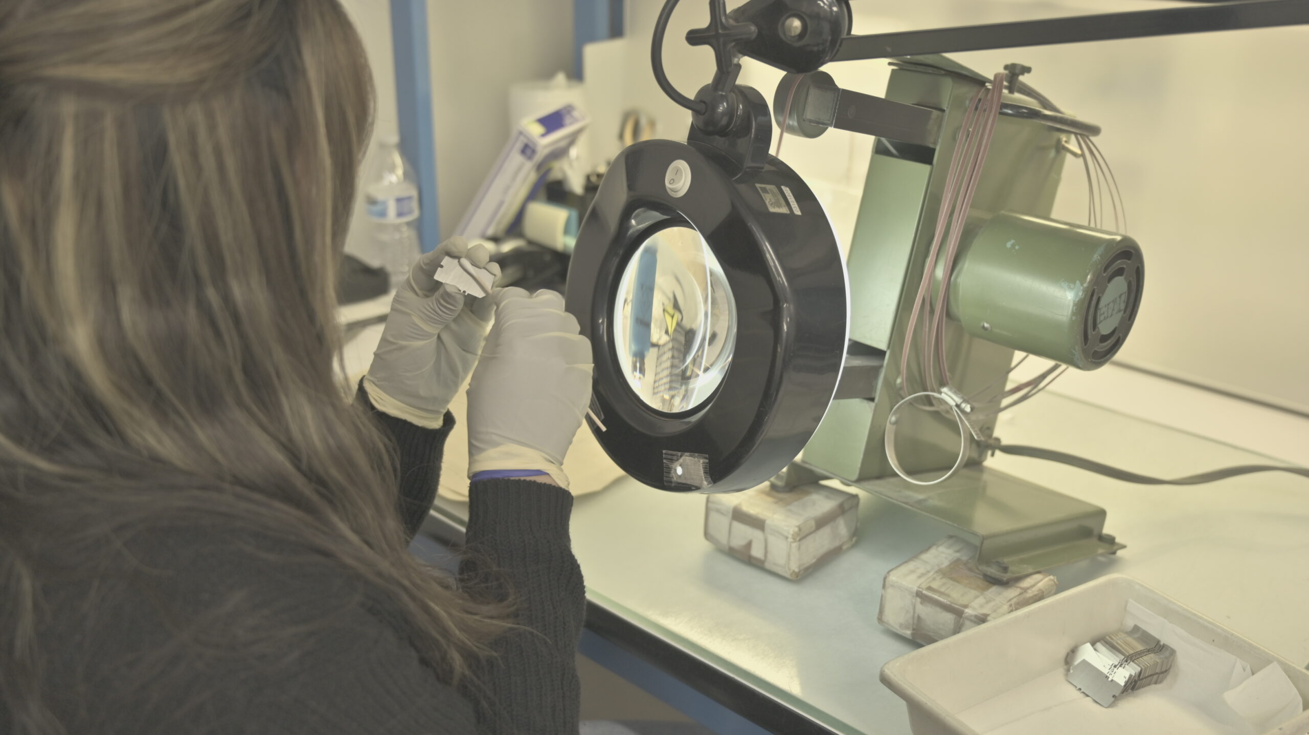
E-Fab Capabilities & Expertise
Our customers choose us not just for what we make, but how we work:
Miniaturization expertise: Mastering tolerances down to microns.
Material handling knowledge: Including expertise in handling silicon-based materials for semiconductor applications, as well as biocompatibility for specialized applications.