The Complete Guide to EMI Shielding/RFI Shielding: Materials, Design & Manufacturing
How EMI/RFI shielding works, how to compare shielding materials, and how precision manufacturing delivers reliable shielding for semiconductor, aerospace, defense, and electronic applications.
Introduction to EMI/RFI Shielding
As electronic systems become smaller, faster, and more densely integrated, electromagnetic interference (EMI) and radio frequency interference (RFI) have become increasingly significant design challenges. From semiconductor manufacturing equipment and telecommunications infrastructure to medical equipment, smartphones, automotive systems, and aerospace electronics in broader aerospace applications, effective EMI shielding is essential for maintaining signal integrity, regulatory compliance, and long-term system reliability.
EMI refers to unwanted electromagnetic energy that disrupts the operation of electronic devices. RFI is a subset of EMI that specifically occurs within radio frequency ranges. These interference sources can originate internally from switching power supplies, processors, high-speed interconnects, and RF circuits, or externally from nearby electronic systems, wireless communications, and industrial equipment. In the worst case, they can cause temporary disturbances, data losses, system failures, and in critical systems, even potential loss of life.
For engineers developing high-performance electronic systems, shielding is not simply a compliance requirement, it is a critical design function.
The effectiveness of any EMI shielding solution depends on three interconnected variables, and practical designs use reflection, absorption, and conductive barriers to prevent interference:
- Material properties
- Frequency of the interference
- Shield geometry and manufacturing precision
Understanding how these factors interact is essential for selecting the right shielding strategy. By combining expertise in shielding materials, electromagnetic performance, and precision manufacturing, E-Fab helps engineering teams develop reliable EMI/RFI shielding solutions for semiconductor, high-frequency, and mission-critical electronic applications.
Why EMI/RFI Shielding Matters in Semiconductor and Electronic Systems
Modern semiconductor equipment and advanced electronic assemblies operate in environments where even minor interference can create performance issues in sensitive devices and compromise information handling.
Common consequences of inadequate shielding include:
- Signal degradation
- Data corruption
- Crosstalk
- Increased noise floor
- Failed EMC testing
- Reduced equipment reliability
- Regulatory non-compliance
In many cases, shielding failures are not caused by the shielding material itself. Instead, they occur at seams, apertures, ventilation openings, grounding interfaces, and mechanically distorted edges, creating additional risk to reliable operation when those features are not controlled.
This is why E-Fab approaches EMI/RFI shielding as both an engineering and manufacturing challenge. By combining material expertise, precision photochemical etching, and tight process control, E-Fab helps ensure shielding components perform as intended in demanding semiconductor and electronic applications.
How EMI/RFI Shielding Works
EMI shielding works by reducing electromagnetic energy transmission and the effects of current flow that couple into susceptible electronics, and engineers use it to protect sensitive components by preventing EMI penetration.
The two primary shielding mechanisms are:
Reflection
Reflection occurs when electromagnetic waves encounter a conductive surface.
Highly conductive materials such as copper, nickel-silver, and beryllium copper create impedance discontinuities that reflect incoming electromagnetic energy away from protected circuitry. Thin metallic coatings can offer shielding on non-metallic enclosures without adding much bulk. Spray-on conductive inks or paints can also be applied to non-conductive casings to create electromagnetic barriers.
Reflection is particularly effective against:
- Electric fields
- High-frequency interference
- RF emissions
Absorption
Absorption converts electromagnetic energy into heat within the shielding material.
Materials with high magnetic permeability absorb magnetic field energy and attenuate low-frequency interference more effectively than highly conductive materials alone.
Examples include:
- Mu metal
- Specialized nickel-iron alloys
- Magnetic shielding laminates
In modern tech, carbon-based absorptive materials such as graphene and carbon nanotubes are also gaining use in EMI shielding because they are ultra-lightweight and corrosion-resistant, though they can be costly and challenging to fabricate.
Most practical EMI shielding solutions rely on a combination of reflection and absorption.
Understanding Shielding Effectiveness (SE)
Shielding effectiveness (SE) measures a shield’s ability to attenuate electromagnetic energy.
It is commonly expressed in decibels (dB):
- 20 dB = 90% attenuation
- 40 dB = 99% attenuation
- 60 dB = 99.9% attenuation
- 80 dB = 99.99% attenuation
Shielding effectiveness testing is commonly performed with specialized equipment in an anechoic chamber or TEM cell using standard methods such as MIL-STD-285, IEEE-STD-299, and ASTM D4935. The shielding effectiveness test (SET) measures attenuation by comparing electromagnetic field strength on the inside to the field strength outside the material or enclosure.
However, shielding effectiveness is rarely determined by material alone.
Shielding performance depends on:
- Conductivity
- Magnetic permeability
- Material thickness
- Frequency
- Aperture size
- Seam integrity
- Grounding quality
- Manufacturing precision
For this reason, material selection without considering geometry often leads to disappointing real-world performance.
Frequency Dependence
EMI shielding performance changes significantly with frequency.
At lower frequencies
- Magnetic fields dominate
- High-permeability materials become important
- Shield thickness becomes more critical
At higher frequencies
- Conductivity becomes increasingly important
- Apertures become major leakage paths, so the opening size should stay small relative to the wavelength at the highest frequency of concern
- Edge quality and enclosure design become critical
This is why the same shielding material can perform very differently depending on operating frequency.
Key Design Considerations for Effective EMI Shielding
Successful EMI shielding starts with design for manufacturability (DFM) from the outset. A concept may look sound in CAD, but still fail if tolerances, fabrication limits, or assembly constraints are not addressed early. Integrating manufacturing insight during the design phase helps eliminate performance risks before testing begins.
E-Fab partners with engineering teams at this stage to refine designs for manufacturability and align material selection with performance requirements. With expertise in photochemical etching and precision metal fabrication, the focus is on delivering shielding components that are practical to manufacture, consistent in production, and optimized for real-world electromagnetic performance.
Even highly conductive materials can underperform when the enclosure geometry is poorly designed.
Shield Can and Enclosure Design
Board-level shield cans and system enclosures serve as the primary containment structures for electromagnetic energy.
Effective designs incorporate:
- Continuous conductive paths
- Minimal seam length
- Controlled grounding points
- Proper ventilation strategies
- Tight dimensional control
Even highly conductive materials can underperform when the enclosure geometry is poorly designed.
Apertures, Seams, and Leakage Paths
Most shielding failures occur at seams and apertures, not through the bulk shielding material.
Common leakage sources include:
- Vent openings
- Connector interfaces
- Access panels
- Assembly gaps
- Fastener locations
- Cable penetrations
As frequency increases, even small openings can behave as unintended antennas.
Reducing leakage often requires:
- Precision apertures
- Tight-fitting interfaces
- Conductive gaskets
- EMI shielding gaskets
- Burr-free mating surfaces
Conductive foam, fabric-covered foams, and interwoven conductive meshes can seal gaps at seams and cable penetrations while maintaining shielding continuity.
Board-Level Shielding Strategies
PCB-level shielding frequently includes:
- RF shield cans
- Component isolation shields
- Partitioned enclosure structures
- Grounded shielding compartments
Board-level shielding may also need filtering on signal lines and display interfaces to reduce coupling into adjacent circuits.
As packaging densities continue increasing, precision becomes increasingly important.
Thermal Management Considerations
Electronic systems generate heat.
Shielding designs must balance:
- Electromagnetic containment
- Airflow requirements
- Thermal dissipation
- Mechanical constraints, since humidity can affect long-term shielding performance through corrosion at vents and interfaces
Ventilation patterns often introduce EMI leakage risks, making aperture design and manufacturing precision particularly important.
Compliance Standards
EMI shielding strategies are often driven by regulatory requirements for wireless communication and medical devices, including:
- FCC standards
- MIL-STD-461
- CISPR requirements
- IEC EMC standards
- CE compliance frameworks
- MIL-STD-285, which specifies shielding-effectiveness test procedures for electronic enclosures
- Aerospace EMC specifications
- Defense electronics requirements
The level of shielding required should be defined early against the applicable standard. Designing for compliance early helps avoid costly redesigns late in development cycles.
EMI Shielding Materials and Their Properties
Material selection plays a critical role in shielding performance.
Common EMI shielding materials also include aluminum, conductive coatings, and conductive elastomers, supporting a wide range of applications. Metal-impregnated plastics are a lightweight, moldable choice, but usually provide lower shielding effectiveness than solid metals.
Different materials provide different combinations of conductivity, permeability, mechanical strength, corrosion resistance, and cost.
Mu Metal
Mu metal is a nickel-iron alloy known for exceptionally high magnetic permeability.
Advantages
- Outstanding low-frequency magnetic shielding
- Excellent attenuation of magnetic fields
- Suitable for sensitive semiconductor and instrumentation systems
Limitations
- Higher cost
- Sensitive to mechanical stress
- Requires careful handling and processing
Typical Applications
- Semiconductor equipment
- Scientific instrumentation
- Medical electronics
- Magnetic field shielding
Steel provides excellent low-frequency magnetic shielding but is extremely heavy, so many engineers select mu metal instead for precision systems.
Beryllium Copper (BeCu)
Beryllium copper combines conductivity with excellent spring properties.
Advantages
- Durable mechanical performance
- High fatigue resistance
- Excellent conductivity
- Reliable grounding interfaces
Typical Applications
- EMI gaskets
- Shield contacts
- RF enclosures
- Telecommunications equipment
It is often paired with conductive elastomers in gasket designs where flexibility and environmental sealing are needed, including particle-filled silicones that use metal particles for effective shielding while maintaining flexibility and environmental resistance.
Phosphor Bronze
Phosphor bronze provides a balance between conductivity, formability, and strength.
Advantages
- Good spring characteristics
- Excellent formability
- Corrosion resistance
- Cost-effective shielding performance
Typical Applications
- Shield cans
- Electronic enclosures
- Grounding components
Stainless Steel
Stainless steel offers mechanical durability and environmental resistance.
Advantages
- High strength
- Corrosion resistance
- Structural performance
Limitations
- Lower conductivity than copper-based alloys
Typical Applications
- Harsh environments
- Aerospace systems
- Industrial electronics
Copper Alloys
Copper-based materials remain among the most widely used EMI shielding materials, with copper, aluminum, and stainless steel being common choices for high-conductivity shielding across various applications.
Advantages
- Exceptional conductivity
- Excellent high-frequency performance
- Broad availability
Typical Applications
- RF shielding
- Semiconductor systems
- High-frequency electronics
Material Comparison Table
| Material | Conductivity | Magnetic Permeability | Relative Cost | Typical Applications |
|---|---|---|---|---|
| Mu Metal | Low | Very High | High | Low-frequency magnetic shielding |
| Beryllium Copper | High | Moderate | High | Shield contacts, RF enclosures |
| Phosphor Bronze | Moderate-High | Moderate | Medium | Shield cans, electronics |
| Stainless Steel | Low | Moderate | Medium | Aerospace, industrial systems |
| Copper Alloys | Very High | Low | Medium | High-frequency shielding |
Frequency vs. Material Selection
Selecting shielding materials without considering operating frequency often leads to ineffective solutions, so engineers must choose materials based on frequency, enclosure geometry, environmental conditions, and the shielding level required.
Low-Frequency Shielding Challenges
Low-frequency magnetic fields are difficult to shield.
These applications often require:
- High-permeability materials
- Greater material thickness
- Specialized enclosure designs
Mu metal frequently becomes the preferred solution.
High-Frequency Shielding Challenges
At higher frequencies:
- Conductivity dominates performance
- Surface currents become critical
- Apertures become primary leakage points
Copper alloys, nickel-silver, phosphor bronze, and beryllium copper are often preferred.
Understanding Skin Depth
Electromagnetic energy concentrates near material surfaces.
Thin conductive foils and coatings can provide strong high-frequency shielding because current is concentrated near the surface.
Skin depth decreases as frequency increases.
As a result:
- Thin conductive materials can provide excellent high-frequency shielding
- Precision geometry becomes more important than bulk thickness
- Manufacturing quality directly impacts performance
Material Selection Guidelines
| Application | Frequency Range | Recommended Material |
|---|---|---|
| Magnetic field shielding | Low frequency | Mu metal |
| RF shield cans | High frequency | Phosphor bronze |
| Shield contacts | Broad spectrum | Beryllium copper |
| Telecommunications systems | High frequency | Copper alloys |
| Aerospace electronics | Mixed environments | Stainless steel or copper alloys |
E-Fab’s Manufacturing Approach for EMI/RFI Shielding
Shielding performance depends not only on design intent, but also on manufacturing execution. Small variations in edge quality, flatness, or feature accuracy can create leakage paths that reduce effectiveness—especially at higher frequencies where seams and apertures dominate performance.
Photochemical Etching (PCM)
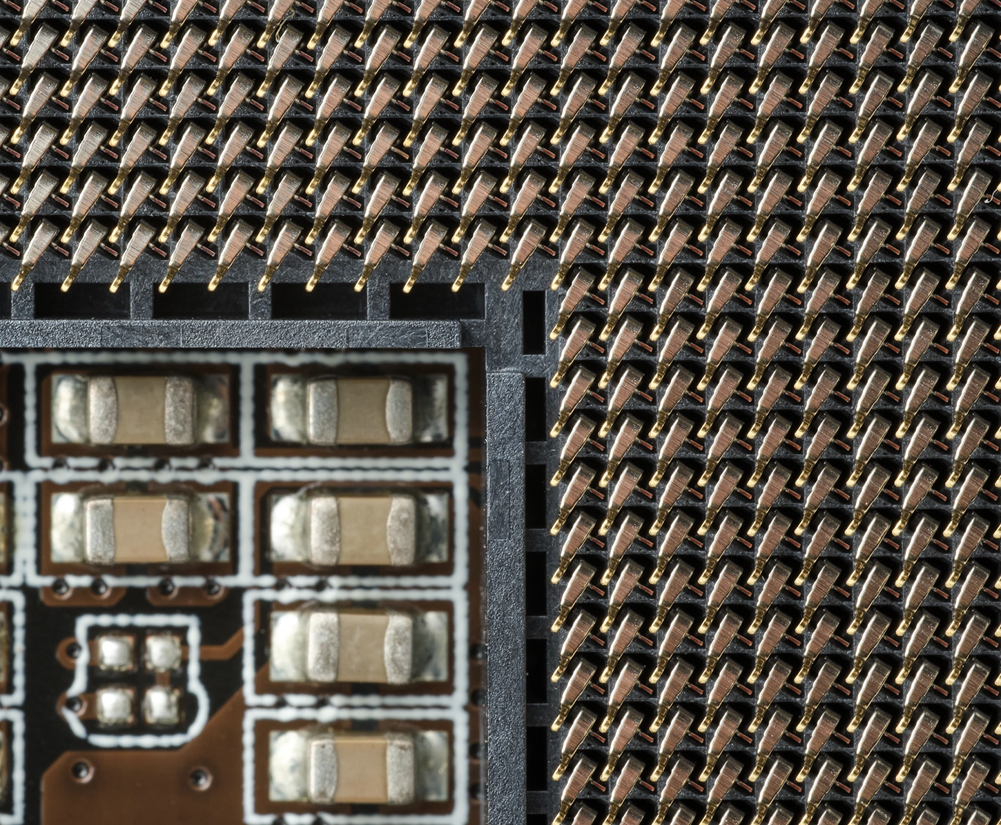
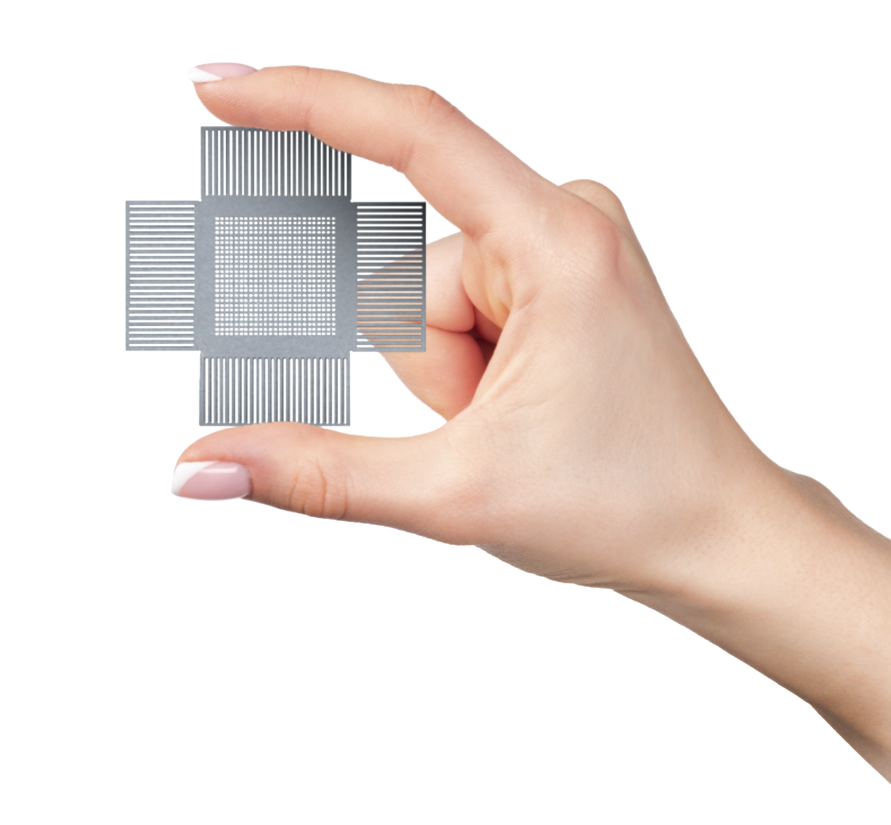
Photochemical etching removes material through a controlled chemical process rather than mechanical force, enabling high-precision features in thin metals without distortion.
Key benefits include:
- Burr-free edges for consistent mating and grounding
- No heat-affected zones, preserving material properties
- No mechanical stress or distortion in thin-gauge metals
- Tight tolerances for high-frequency applications
- Complex geometries and fine features without deformation
- High repeatability for scalable production
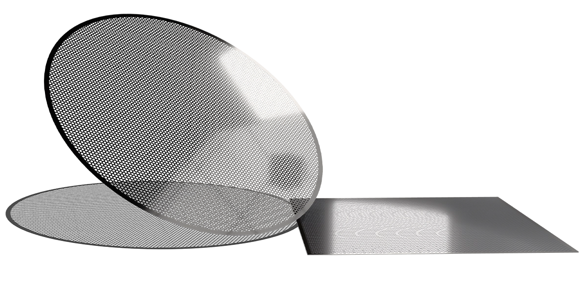
For EMI/RFI shielding, PCM is particularly effective for precision apertures, vent patterns, and intricate shield geometries where edge quality and dimensional control directly impact shielding effectiveness.
Hybrid Manufacturing with Custom CNC Machining
To extend design flexibility and support photochemical etching efficiency, E-Fab integrates custom CNC machining for complementary features that go beyond planar etching.
This includes:
- Secondary forming and precision finishing operations
- Structural or 3D features beyond PCM capability
- Tooling and fixture support for repeatable builds
- Rapid prototyping and design iteration support
Together, PCM and CNC machining provide a balanced approach—combining high-resolution feature control with structural versatility while improving manufacturability and reducing design constraints.
Why Photochemical Etching Is Ideal for EMI Shielding
As frequencies increase and packaging densities shrink, precision manufacturing becomes increasingly critical.
Photochemical etching helps address common shielding failure modes:
- Burr-free edges eliminate inconsistent mating surfaces, grounding variation, and gap-induced leakage
- No thermal processing avoids distortion, metallurgical change, and residual stress
- Tight tolerances support precision apertures, fine meshes, and controlled vent patterns
- Complex geometries enable compact, lightweight shielding structures without mechanical deformation
These capabilities support consistent shielding performance in thin-gauge metals used for high-frequency and semiconductor applications.
Rapid Iteration from Prototype to Production
PCM also enables fast design validation, allowing engineering teams to identify EMI issues early and refine shielding designs without disrupting production consistency. This supports a smooth transition from prototype builds through full-scale manufacturing while maintaining repeatability and process control.
EMI/RFI Shielding Applications
Aerospace and Defense Electronics
Critical systems require shielding solutions capable of meeting stringent reliability and compliance requirements for safety reasons.
- Radar systems
- Avionics, including navigation and communication systems
- Electronic warfare systems
- Secure communications
High-Frequency Electronics
- High-speed digital systems
- RF modules
- Mixed-signal electronics
- Advanced computing platforms
- Mobile phones and other compact RF devices, where shielding helps control emissions and protect dense mixed-signal layouts from RF waves
Semiconductor Equipment
- Process control electronics
- RF power systems
- Sensor protection
- Wafer processing equipment
Telecommunications Systems
- Base stations
- Network infrastructure
- Satellite communications
- RF amplifiers
Medical and Industrial Electronics
- Diagnostic equipment
- Imaging systems
- Industrial automation
- Precision instrumentation
How E-Fab Supports EMI/RFI Shielding Projects
At E-Fab, we provide precision-manufactured EMI shielding components for semiconductor, telecommunications, aerospace, defense, and advanced electronic systems. The difference is we’ve devoted more than 40 years into honing our craft and sharing our knowledge with our clients.
Our capabilities include:
- Material selection guidance
- Precision photochemical etching
- Shield can manufacturing
- EMI shielding gaskets
- Fine-feature apertures and meshes
- Forming and fabrication services
- Bonding and assembly support
- Plating capabilities
- Prototype-to-production scalability

We manufacture shielding components using:
- Phosphor bronze
- Beryllium copper
- Mu metal
- Nickel-silver
- Stainless steel
- Copper alloys
Engineers also have experience with particle-filled elastomer options such as silver, copper, and nickel-graphite where sealing and conductivity must be balanced.
Engineers rely on E-Fab when shielding performance depends on:
- Tight tolerance control
- Repeatable manufacturing
- Complex geometries
- Burr-free edge quality
- Consistent electromagnetic performance
Additional advantages include:
- ITAR-cleared manufacturing support
- Collaboration with engineering teams
- Support for EMI/RFI validation initiatives
- Reliable production quality backed by process control and repeatability metrics
The result is a shielding solution optimized not only for material performance, but also for manufacturability, reliability, and long-term production success, with E-Fab helping customers select the right material and process for a wide variety of enclosure and gasket designs.
Frequently Asked Questions About EMI Shielding
What is the difference between EMI and RFI?
Engineers also have experience with particle-filled elastomer options such as silver, copper, and nickel-graphite where sealing and conductivity must be balanced.
What determines shielding effectiveness?
Shielding effectiveness is influenced by material conductivity, magnetic permeability, thickness, enclosure geometry, seam integrity, grounding quality, frequency, and manufacturing precision. The required shielding level typically depends on the application, operating environment, and applicable compliance standard.
What causes most shielding failures?
Most failures occur at seams, apertures, vent openings, connector interfaces, and grounding discontinuities rather than through the shielding material itself.
Which material is best for EMI shielding?
The best material depends on frequency range, field type, environmental conditions, mechanical requirements, and enclosure design. There is no universal shielding material for every application. The right choice also depends on weight, sealing needs, and whether magnetic materials or conductive elastomers are required.
Why is photochemical etching used for EMI shielding components?
Photochemical etching produces burr-free, stress-free components with tight tolerances and complex geometries that help improve shielding performance, particularly in high-frequency applications.
Request a Quote for Precision EMI/RFI Shielding Components
Effective EMI shielding requires more than selecting a conductive material. Performance depends on the interaction between material properties, operating frequency, enclosure geometry, and manufacturing precision.
E-Fab helps engineering teams develop EMI shielding solutions optimized for semiconductor equipment, telecommunications systems, aerospace electronics, defense applications, and other high-performance electronic systems.
Discuss your EMI/RFI shielding requirements, material options, and manufacturing specifications.
Evaluate design considerations, material selection, and photochemical etching strategies for your next shielding project.