
And Why Now Is the Pivotal Moment for U.S.-Based Semiconductor Manufacturing
The semiconductor manufacturing industry is at a history-defining moment. Global supply chain disruptions, mounting geopolitical pressures, and new policy frameworks, such as the U.S. CHIPS Act and recent tariffs on non-U.S. semiconductor imports, are redefining how and where critical components should be sourced. Decision-makers in engineering, procurement, and R&D are increasingly recognizing that sourcing domestically is no longer just an option, it’s a strategic necessity. However, establishing a new fab in the U.S. presents significant challenges, as the costs are much higher compared to Asia due to lower government incentives and support.
Against this backdrop, U.S.-based manufacturers like E-Fab are stepping up to deliver not only security and reliability but also world-class precision. For semiconductor leaders, creating resilient and innovative manufacturing capabilities is essential to keep pace with the world’s leading chip production regions, such as South Korea and Taiwan. Choosing the right partner isn’t just about keeping the supply chain moving, it’s about safeguarding intellectual property, accelerating innovation, and staying ahead in an intensely competitive semiconductor production market.
The State of the Global Semiconductor Industry
It’s important to highlight that the global semiconductor industry is far more dynamic and competitive than ever before. With demand for advanced chips and microelectronics surging across sectors from automotive to cloud computing, the pressure on semiconductor manufacturers to deliver high-performance, reliable devices is at an all-time high. Regions like South Korea and Taiwan have long been at the forefront of chip manufacturing, leveraging cutting-edge semiconductor manufacturing equipment and highly specialized wafer processing techniques to produce the world’s most advanced silicon wafers and individual chips.
However, this global dominance comes with challenges. The semiconductor manufacturing process is incredibly complex, involving multiple steps such as chemical vapor deposition, ion implantation, thin film deposition, and both wet and dry etching to create intricate circuit patterns on each wafer surface. Several companies must coordinate across continents to source materials, manage wafer fabrication, and assemble working chips, making the entire production process vulnerable to disruption.
As the world’s appetite for new technology grows, so does the need for a resilient, secure, and innovative semiconductor supply chain, one that can keep pace with rapid advances in chip design, wafer processing, and the creation of next-generation semiconductor devices.
Strategic Advantages for U.S.-Based Sourcing
Choosing a U.S.-based semiconductor manufacturing partner provides advantages that directly impact performance, reliability, and quality:
- Shorter, more reliable lead times – Reduce uncertainty by eliminating overseas shipping delays and port congestion.
- Enhanced IP protection – Keep your designs secure with fully domestic design, prototyping, and production.
- Better regulatory alignment and higher quality assurance – Meet strict U.S. standards and compliance requirements with confidence.
- Access to government incentives – Leverage U.S. programs designed to strengthen domestic semiconductor production. Organizations like Applied Materials play a key role in providing advanced equipment for domestic semiconductor manufacturing.
Simply put, sourcing in the U.S. is about more than convenience, it’s about protecting your competitive edge. A company can also benefit from projected improvements in supply chain reliability and product quality by sourcing in the U.S.
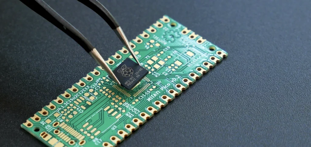
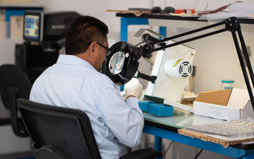
E-Fab’s Unique Semiconductor Manufacturing Process Capabilities
What sets E-Fab apart is not just that we’re U.S.-based, it’s that we bring unmatched precision, speed, and materials expertise to every project:
- Photochemical etching with micron-level tolerances – Achieving stress-free, burr-free parts with unmatched accuracy. Our precise patterning and etching processes ensure that features are accurately formed, defects are minimized, and each layer is defined to exact specifications.
- Versatility in materials – From copper and stainless steel to exotic materials like molybdenum, titanium, Invar, and Kovar. We have deep expertise in depositing and handling advanced material layers, supporting the complex requirements of semiconductor manufacturing.
- Rapid prototyping to high-volume production – Seamlessly scaling from design iterations to full production runs without compromising quality. We maintain the integrity of deposited layers and minimize defects throughout the manufacturing process.
This combination ensures our customers receive semiconductor manufacturing components engineered with precision, reliability, and speed, with every component precisely formed, etched, and patterned to meet the highest industry standards.
Actual Semiconductor Equipment Components Produced by E-Fab
E-Fab delivers a broad range of semiconductor production components that demand exacting standards:
- Lead frames – Micron-precise copper and alloy frames for device mounting. These frames also serve as substrates for mounting chips in electronic devices, providing a stable platform for electrical connections.
- EMI/RFI shielding – Thin, complex shields to protect RF-sensitive modules.
- Interconnects and contact elements – Designed for superior conductivity and alignment.
- Thermal management parts – Heat exchanger plates, heat sinks, and other solutions for effective dissipation.
- Masks, apertures, and carrier plates – Essential for lithography, wafer handling, and secure component mounting. These components are patterned using photoresist during lithography to achieve the intended circuit pattern, ensuring precise feature definition on the wafer.
- Other thin metal components – busbars, flexure springs
Each component reflects the high level of craftsmanship and technical rigor that E-Fab brings to semiconductor manufacturing.
Prototyping Excellence: From Concept to Semiconductor Device Component
Time-to-market can make or break a semiconductor innovation. That’s why E-Fab specializes in rapid prototyping, helping engineers move from design concept to functional component in record time. Our process supports quick design iterations, shorter development cycles, and greater design flexibility. During prototyping, we often work with silicon wafers and employ techniques such as wet etching or the use of specialized gases to achieve precise feature definition.
There Is No Better Time Than Now
In today’s semiconductor manufacturing landscape, U.S. operations aren’t just advantageous, they’re essential. With E-Fab’s precision-engineered solutions, rapid prototyping expertise, and secure U.S.-based facilities, we provide unmatched value for semiconductor leaders looking to protect their IP, strengthen their supply chain, and speed innovation.
Partner with E-Fab, the trusted U.S. source for precision semiconductor components and truly made in the USA electronics.
See our capabilities and contact us today to explore how E-Fab can accelerate your next semiconductor production breakthrough.